Battery Top Signal Generator
© Brooke Clarke 2006

Background
Description of the BTSG
ICS525 Description
Choosing an Input Frequency
Pushing the Limits
Related Products
Links
Ordering
Background
ICS
(now merged into
IDT) developed the
525 series of User Configurable Clock chips all available only in the
fine pitch SOIC-28
Surface Mount
Package.
This is a single chip that contains a PLL including prallel controlled
dividers on the input, the VCO and the output. Getting the
factory demo board proved expensive and had very long lead time so I
made my own but with different features.
Feb 2008 - Although this device will provide a signal suitable for say
testing if a receiver is working, it's not going to do a good job if
you want to use it for a crystal replacement in a radio. That's
because there is a lot of jitter and phase noise. By choosing
numbers so that the output divisor is maximized the jitter is reduced
more than for other number sets, but still not good enough for radio
crystal replacement.
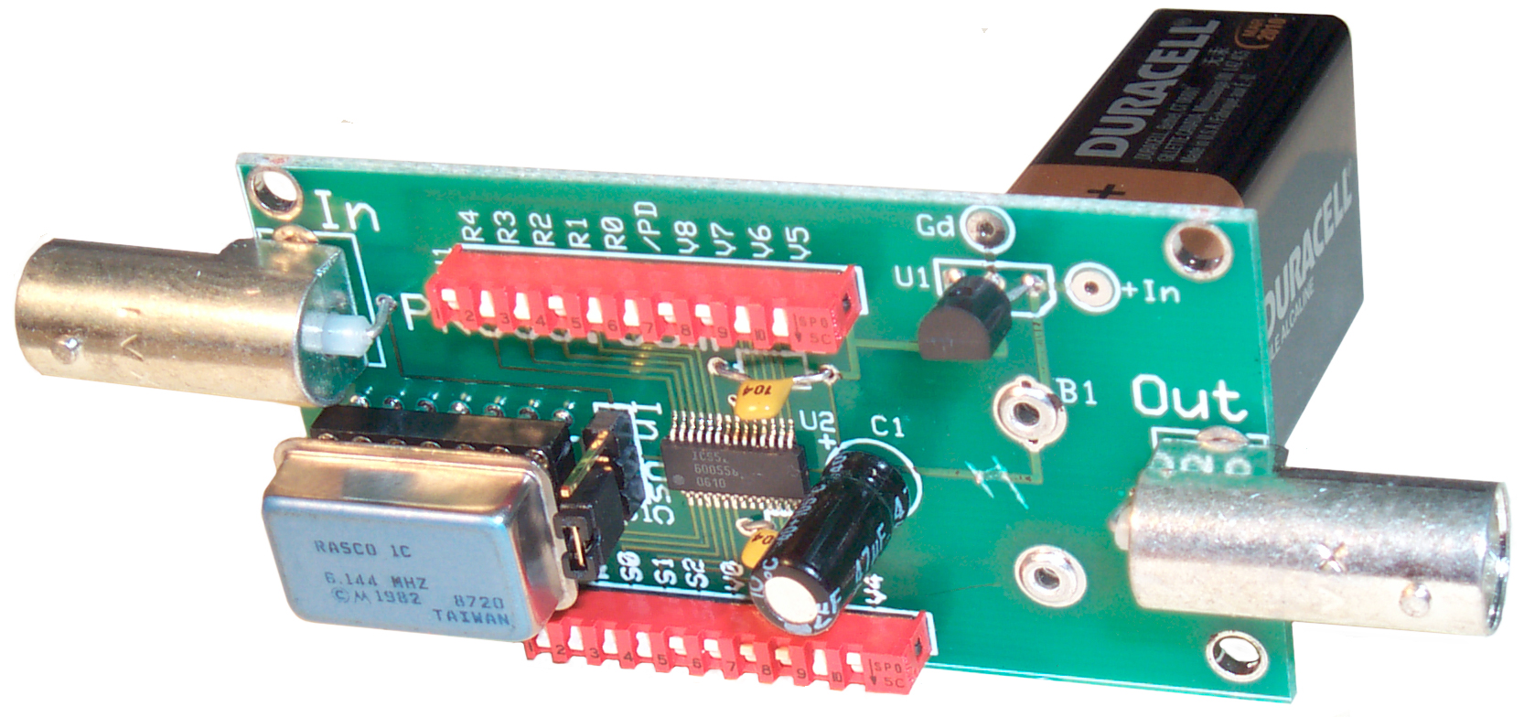
Description of the BTSG
Features of the BTSG
- Version 1 uses the 525-02 which is faster than the -01
- Uses SIP switches to program the dividers and turn unit on and off
- Jumper choice of using BNC input or on board DIP oscillator
- DIP oscillator socket supports either full or half size packages
- Output on BNC connector
- On board 5 Volt regulator fed from either 9 volt battery snapped
to back of board or
external DC supply
- When a battery is attached the board stands up like in the photo
above. Then switch up = 1 down =0 to match the ICS calculator
table
Can be used to generate "even" frequencies from the color burst
frequencies. For example a 4 times color burst DIP oscillator at
14.31818 MHz will exactly provide 1, 5, or 10 Mhz. And vice versa
a 10 Mhz standard will generate 1, 2 or 4 times color burst exactly.
ICS 525 Description
The output frequency is given by:
Fout = Fin * 2 * (V+8) / ((R+2) * S)
V, the 9 bit VCO divider, and R, the 7 bit Reference input divisor, are
straight binary but S needs to be looked up in a table:
Divisor
|
Switch
Bits
|
1
|
110
|
2
|
001
|
3
|
111
|
4
|
011
|
5
|
100
|
6
|
000
|
7
|
101
|
8
|
010
|
A convenient way to get the divisor
values is to use the
ICS on
line calculator but be sure to scroll down to the 525-02 results,
don't use the -01 results. In the first table under ICS525-02
note that VCO divider is the actual divisor, ref divider is the actual
input divider and OD is the Output Divider. VDW and RDW are the
switch values which have been offset by 8 and 2 respectively.
In the next table there are typically 3 results diplayed Best Accuracy,
Lowest Jitter and Lowest Idd. Let's look at an example:
Vdd = 5 Volts
Input frequency = 16.6666 MHz
Output frequency = 80 MHz
Table 1 shows the actual VCO, Ref and Output divisors and I've added
some more calculated data
|
error
ppm
|
VD
|
RD
|
OD
|
Fvco
Fo*OD
|
Ph Det
Fvco/VD
|
| Best Accuracy |
0
|
36 |
3 |
5 |
400
|
11.1111
|
| Lowest Jitter |
0
|
24 |
2 |
5 |
400
|
16.6666
|
| Lowest Idd |
0
|
12 |
5 |
1 |
80
|
6.6666
|
My guess is that:
- Best accuracy is based on the error for those cases where there
is an error and then on highest VCO divisor for those cases like this
where there is no error.
- Lowest Jitter is based on the highest Output Divisor and when
there's a tie on the lowest VCO divisor.
- Lowest Idd is the lowest VCO frequency.
Choosing an Input Frequency
Since the PLL works using integer
divisors on the Reference input, VCO and output it's good if you can
choose an input frequency that has factors that divide to get you to
the phase detector. For some common crystal and oscillator
frequencies and their prime number factors see my
Crystal Frequency web page.
Pushing the Limits
Max Fout 525 MHz
In the above example note that the first two choices have the VCO
running at 400 MHz and the Output divisor at 5. If the output
divisor is changed to 1 (code 110) then the output is 400 Mhz. Maybe
there's some problem with
temperature? This is higher than the data sheet Fmax value of 250
MHz. The input frequency can be reduced with the 24-2-1 divisors
down to 120 kHz with an output near 2.8 MHz, but very noisy.
When the input frequency is raised from 16.6666 to 20.766 Fout goes up
to 500 MHz and there my spectrum analyzer quits. Using a receiver
I can detect signals up to 525 Mhz without any direct connection.
By choosing the input frequency to be as low as possible the VD value
will be maximized thus minimizing the step between adjacent programmed
outputs.
Min Fout 360 kHz
By setting the VCO divisor to it's min value and the Ref and Output
divisors to their max values results in the lowest output frequency for
whatever is the input.
Fout = Fin * 2 * (0+8) / (127+2) * 8) = Fin /64.5 This did not
work.
But using OD=8, VD=18 and RD=5 causes Fout = Fin * 0.9 and works down
to Fin = 400 kHz and Fo = 360 kHz.
Data sheet says phase detector freq 200 kHz min, but in the above case
it's 80 kHz so they have some margin.
Related Products
Battery Top Power
Supply -
tvb Divider - this divider will take
in a 10.0 Mhz signal and output all the decades from 100 kHz down to
1,000 seconds per pulse. The input can be any frequency from near
DC to 20 Mhz. So be using the BTSG to change a precision 10
MHz signal to something a little lower, like 4.4 MHz (which can be done
with zero error) then the tvb divider will change that into a 440 Hz
square wave of very high precision.
Links
TAPR
Clock-Block - Phase Noise plots for the ICS525
Ordering
There are a couple if issues that
needed to be worked out with the factory then these will be available
on a trial basis.
Back to Brooke's Military
Information, Electronics,
Home page
This is the [an error occurred while processing this directive] time
this page has been accessed since since 14 May 2005.