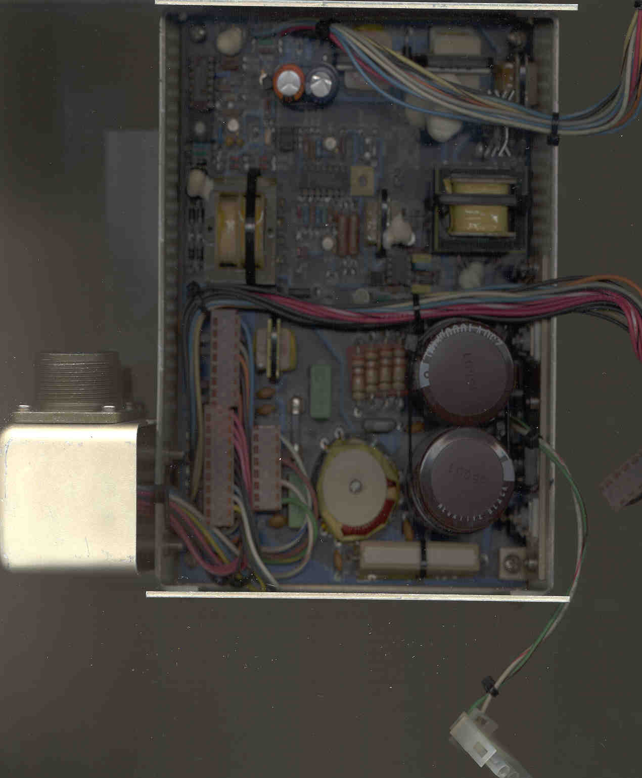
Across the top are Test Points for:
RPT6041.DWF
To view this file you need to use the free WHIP! plug in from Autodesk.115/230 to 300 VDC
It takes in the 115 or 230 volts and converts it into 300 VDC. This is done in the input side clam shell of the dual clam shell power supply. Because there is no mains frequency transformer the power supply appears to be DC open when the line cord is tested with an ohm meter.
There is 318 VDC going to the output half of the supply indicating that the first half is OK.300 VDC Switch to -12
All the outputs are supposed to operate with no load with no more than a 5 % increase in output voltage. When J2 is disconnected, removing all loads, the -12 Volt supply seems to work OK.300 VDC Switch to +24
The +24 VDC supply has no output. Since it feeds the +5 and +12 outputs they are also dead.
Q3 is extremely hot. It is markedBUZ71AThe schematic shows it as
PH
8630
G D SQ3It is the switch that drives T2 through D4 (4937). The source is connected to ground. The Gate is driven from a 7556 dual timer. The Drain is connected to the +24 VDC output. T2 drives the gates of Q1 & Q2 (IRF840R) which are the main +24 VDC switches to T1. U2 is a 723 high quality linear power supply chip. U1 (LM139 op amp), U2 and U3 are feed from the Sheet 2/6 portion of the supply that includes the -12 volt supply.
71AU2 (723) has a 5.1 V zener connected from pn 7 (V-) to pin 2 (ILIM) and with the chip out of it's socket the voltage is about 5.5 VDC, but with the chip installed it's about 1.8 VDC. Maybe the 723 is dead?
+24 VDC Linear to +5 VDC
+24 VDC Linear to +12 VDC
The RCS-5A receiver is totally dead.
 There
is a 17(f) pin socket MS connector {A18-J2] and a 5(m) pin MS connector
[A18-J1] to the right of this image.
|
|
|
|
|
|
|
|
|
|
|
|
|
|
|
|
|
|
|
|
|
|
NC | NC |
|
|
|
Set Voltage |
|
|
|
|
|
|
|
|
|
|
|
|
|
|
|
|
|
|
|
|
|
|
|
|
|
|
|
|
|
|
|
|
|
|
|
|
|
|
|
|
|
|
|
|
|
|
|
|
|
|
|
|
|
|
CRT&MB |
|
|
|
|
|
|
|
|
|
|
|
|

Across the top are Test Points for:
|
|
|
|
|
|
||
|
|
||
|
|
|
|
|
|
|
|
|
|
|
|
|
|
|
|
There are 4 cables leading from the first clam shell.
The 12-pins at the top right are P2.
The dual 12-pin (24 total( verticle in the center is P4.
One cable goes to the 3-pin molex connector P3 (along bottom edge of
this view and has the two wires carrying the 300 Volts DC from the first
half.
|
|
|
|
|
|
|
|
|
|
|
|
|
|
|
|
|
|
|
|
|
|
|
|
|
|
|
|
|
|
|

The Input side has a metal box holding J1 and J2, the 300 Volt DC supply
and some of the output voltage supplies.
This box contains U14, U15, U16 and U17.
The Yellow transformer along the right wall is T12 which is driven from
U17
|
|
|
|
|
|
|
|
|
|
|
|
|
|
|
|
|
|
|
|
|
|
|
|
|
|
|
|
|
|
|
|
|
|
|
|
|
|
|
|
|
|
|
|
|
|
|
|
If all the boards are removed from the motherboard ( A9, A10, A11, A12,
and A13) and all the power connectors are removed from A4, A5, A6 and A7
then the -12 VDC output can be adjusted and appears OK. If any of
the boards is connected the voltage drops from -12 to around -8 and with
all connected the voltage drops to around -4 VDC. Transformer T12
is driven from Q42 which is driven from U17 (Cherry
Semiconductor CS-2842A).
With the power supply outupt connector (J2) disconnected the frequency
from U17 #7 to "300R" is about 7 kHz and with J2 connected (all loads applied)
about 13 Hz. The dsata sheet for the CS-2842A indicates for Rt=649
Ohms and Ct= 15 nF the frequency should be about 76 kHz. Vcc at U17
#7 is about 10.95 with J2 connected and with J2 disconnected the voltage
varies from 10 to 13 VDC. Pin 8 Vref should be 5.0 VDC but it is
around 2 volts. I think that U17 is bad.
U17 was not the problem.
Q3 is extreamly hot.
Q3 the BUZ71A, U2 the LM723CN and U3 the NE556 are all available form
ST
Microelectronics in San Jose.
Possible inventions:
US4009430: Antiparallel commutated inverter Feb. 22, 1977 / April 14, 1975 issued/filedback to Brooke's RCS-5, home page
US3925633: Circuit for controlling power flow from a high frequency energy source to a plurality of high frequency loads Dec. 9, 1975 / Sept. 6, 1974
US3652874: CIRCUIT FOR CONTROLLING THE CONDUCTION OF A SWITCHING DEVICE March 28, 1972 / July 30, 1970