In this method the larger components are mounted on a chassis and controls are mounted on the front panel. Smaller components are connected directly between those already mounted. Where an intermediate tie point is required a terminal strip is mounted to the chassis. A terminal strip is a piece of phenolic with one or more terminals pointing up and all insulated from each other. There's at least one attachment point which has a terminal at the top for a chassis ground connection and at the bottom there's a foot with a screw hole so that terminal strip can be attached to the chassis.
In this technique the assembly line is linear, that is to say all the mechanical work, paint and labeling must come before any electrical assembly.A "bread board" was literally made using a wooden board used for kneading bread dough.
This was the method used for all electrical construction up to the 1950 time period. The active devices were vacuum tubes. The filament power of a tube needs to be about the same as the output power rating so that tube devices always have an energy efficiency of less than 50%, sometimes way less. I knew a man who worked for RCA and his job was to design color TV picture tubes so that they would fail just after one year (the common warranty period). I think that vacuum tubes were also designed to have a 1 year operational life so that you would buy more tubes. Every drug store had a tube tester with the common consumer part numbers in the base. I made many trips there with a paper bag filled with tubes, one of which would be found dead.
A common pilot lamp setup was to use a faceted glass window through the front panel mounted to a socket which held a number 47 lamp. This was powered by the filament winding of the power transformer. When lit you knew that the line fuse was OK and the transformer was putting out filament voltage. Another option was to use a Neon lamp, but these were not as bright and could not be filtered to give many different colors, but they did not burn out like the filament style lamps.
If you connect a 90 Volt battery in series with a resistor and then connect a Neon lamp and capacitor to ground you get a relaxation oscillator. The RC circuit charges up and when the voltage gets to the Neon firing voltage the Neon lights and pulls charge from the capacitor. Once the voltage gets below some value the Neon lamp goes out and you wait for the next charge time. The effect is to have a lamp blinking all the time and mine was about once per second.
Radio receivers built in this time frame did not have enough frequency accuracy to tune to a station, you needed to tune above and below the indicated frequency until the station was found. You could not just tune to the correct frequency and wait to hear it. Once the station was heard you could record the logging dial setting which typically was a number between 0 and 100 on the band spread dial.
This is an extension of the terminal strip. It consists of an insulating board (Masonite, phenolic, etc.) about 2 inches high and maybe 6 inches long (varies with what is on it). There are terminals along both long edges with components mounted between the terminals and one or more wire cables leaving that are pre shaped and cut to length. This board can be assembled and tested prior to any chassis hardware being available, shortening the span time on the assembly line.This was used for vacuum tube and some germanium transistor equipment. Early HP equipment used terminal boards, for example see the HP 415A Fig 5.
This is an extension of the terminal board where a layer of Copper is added to the terminal board that can be etched to replace the component to component wiring and the terminals can be replaced with holes for the component leads "through hole construction". A number of the components need to have new form factors for direct mounting to the PCB. Television sets made using tubes and PCBs had failures when the heat caused the cheap FR4 FR2, similar to NEMA grade XXXP (MIL-P-3115) boards to crack opening traces.Soldering all the connections after the board is stuffed is time consuming and error prone. Wave soldering was developed to solder all the joints in a very short time. A common costing method was to count the number of holes in the board. This lead to more functions in a circuit package to minimize the number of pins.
Silicon transistors and early integrated circuits (IC) used this method. The pin spacing on early Dual Inline Plastic (DIP) ICs was 0.1". This made for a standardized 0.1" grid for PCB layout.
When it was desired to connect a test instrument to a PDP-11 core memory computer, or other device for remote control, connectors were added to the back with a wire for each switch contact on the front panel or each "bit" of data. This required connectors with large numbers of contacts and a customized card in the computer for each instrument. One of the control positions would correspond to all open switches or a separate local-remote switch was used to lift the common switch connections thus allowing the remote to function independent of the mechanical switch positions. When being remotely controlled these instruments typically would not show any indication on the front panel of what was going on.
HP developed HP-IB (later IEEE-488, later GP-IB) as a standardized way to remote control instruments. It has a handshake scheme so that the slowest instrument gets it's data before the next parallel 8 bit byte is sent. There are also a number of dedicated control lines.
2699425 Electroplating electrical conductors on an insulating panel, Nieter Temple, Motorola, App: 1952-07-05, - silk screen process
Initially the components were laid down on a single board. With cord wood construction the components are mounted between two boards. This results in a much smaller and more rugged assembly.
3027627 Encapsulated miniature electrical circuits, Robert H Sturdy, C K Components, App: 1959-05-28, Pub: 1962-04-03, -
This is a simple extension from single sided PCB but requires a way to connect traces on opposite sides of the board. I worked with some early DS PCBs and we used a shoe eyelet machine to install eyelets (like very small rivets except they have a hole through the center).
Later a reliable "via" was developed so that a PCB board shop could plate through the via holes.
3194681 Process for plating through holes in a dielectric material, Richard J Nicholson, Robert P Williams, NCR Corp, App: 1960-12-22, Pub: 1965-07-13, -
A version of this is called "cord wood" where instead of mounting components to a single board they are mounted between two boards. This results in a very dense packing of the components and allows non planar shapes, like a hollow cylinder to be made. The RS-49 was the first CIA made radio to use this method and that was in the 1963 - 1964 time frame (they called it "sandwiched"). The GRA-71 keyer uses cord wood.
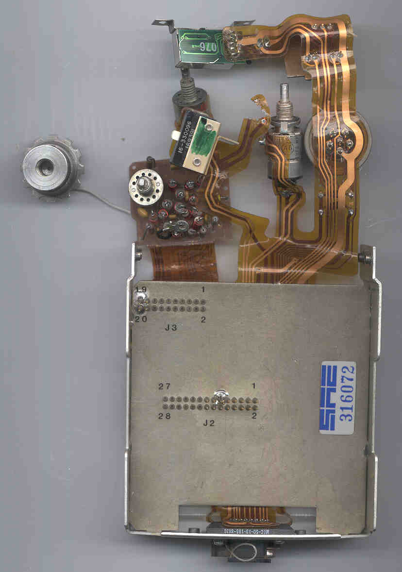
Another version of this is the flex circuit. Instead of using FR4 or fiberglass for the board material a thin flexible plastic is used. This is great for things like wiring the controls on the panel of a PRC-68 radio.
Yet another version is "Chip On Board" (COB) where the semiconductor die is attached directly to the board. It could be with the bonding pads up and conventional wire bonding used to connect between the board and the chip. It could be a bumped chip where there is a solder drop on each bonding pad and the chip is soldered to a flex circuit. The flex circuit and chip are cut out and the flex circuit attached into a package or to a board. This is used for things like greeting cards and other low cost high volume applications.
Bread boarding and small run prototyping could be done using wire wrap technology. The component side of one of many PCBs lookes like this Stanford Telecommunications 5001 GPS simulator board. This instrument is serial number 4.
Another option was to make a PCB by making a 4X trace layout using Mylar grid paper and black tape with special "donuts" for the component holes and have life size a litho negative made. The PCB shop would use this to etch the board. Double sided boards required alignment marks on each negative done is such a way that they would not be used flipped or reversed.
This method was used for Silicon transistors and was very popular for ICs. Multi-function ICs and early Application Specific Integrated Circuits (ASIC) used this method. A PCB with hundreds of general purpose ICs could be replaced by a single board with just a few ASICs greatly reducing the number of holes and therefore the cost. Since ASICs are not general purpose, repairs become harder if not impossible.
Nuvistors were tubes made using ceramic cylinders instead of the conventional vacuum tube glass bulbs. They could run on lower voltages and were promoted as an alternative to transisitors by some tube manufacturers.
Remote control was by means of RS-232 or HP-IB (IEEE-488, GP-IB) interface. The controls were no longer mechanical point to point but instead momentary contact switches (normally open) with some type of indicator to show the state of each switch.
HP developed 10Base-T, a way to use existing premises wiring for computer networking as a much lower cost alternative to installing coax cables. This developed into 100Base-T (CAT5) and higher speed versions that need special Unshielded Twisted Pair (UTP) cabling.
Many things were made using general purpose parts that could be repaired. These are in my opinion the "Golden Era" products because they can be maintained almost forever. When a newer design fails the only option is to get replacement modules form the factory, and if the factory is no longer selling them it's very difficult or impossible. There are a few parts in the PRC-68 series radios that are ASICs or programmed microcontrollers that can not be purchased new now, but most of the rest of the radios are made from general purpose parts and are repairable.
Some PRC-68 radios were made using two double sided boards separated by 1/16". At that time miltilayer boards were not available.
The Austron 2100F LORAN-C Frequency Monitor and 2100T LORAN-C Timing Receiver use double sided Printed Circuit Boards and have documented HP 5004 Signature Analyzer data to aid in troubleshooting to the IC level. This is probably the last of the equipment designed so that individual ICs can be replaced. After this troubleshooting is done by the board swap method or even equipment swap, like for a modern TV set.
Once a via can be made, it's a natural extension to make a PCB with multiple layers which is how computers and other complex electronics boards are made now.Complete function on a chip packages are used with this method as well as all of the above. It is impossible to repair a multiple layer board and even replacing a component can be extreamly difficult or impossible depending on the packaging method. Most of these are replace instead of repair.
Vacuum tube technology developed so that a tube would last as long as a transistor. The PRC-25 Viet Nam vintage radio has a final 2D24 tube thats known to never fail under normal conditions.
Later versions of the PRC-68 use a single multilayer PCB instead of the two seperate baords.
ExpressPCB offers 4 layer boards where the center two layers are always power and ground planes. The top and bottom layers are normal user wiring. The capactance between the power and gound planes is a good thing. Also both power and ground planes are connected by capacitors so both are good RF grounds which is a good thing if you need to meet FCC radiation standards. Whenever there's a hole from the top to the bottom that should not connect to either power or gorund, the center layers have a hole in the metal patters so that the via will not make electrical connection to the center layers. It's much easier to layout a 4 layer board since there's no power traces to work around.
Back to Brooke's Hints & Tips (or What goes wrong), PRC68.COM, Military Information, Electronics, Home page
[an error occurred while processing this directive] page created 6 July
2001.