FS-5000 Spy Radio
© Brooke Clarke 2004 - 2012
Description
Purpose & Use
Millitary Collector Group Post
Boxology
Major Components
Accessory Kit Contents
X Box
H Bar
Receiver Synthesizer
Digital Data
Bottom Digital
PCB
Synthesizer
DB15 connector
between Bottom and Top of Rx
Central IF PCBs
Top RF & Mixer
PCB
No micro
controller
Transmitter Controller
HFS7000
Radio and TCU7000 Control Box
DB-25
Interface Connector
20 Nov 2004 New Theory about
F0, F1, F2 & F3
21 March 2005 - Remote Rx Freq
Procedure
28 March 2005 - Tx with Ant
Coupler Proc (no Modulation)
3 April 2005 - Rx & Tx
controlled using PC Basic program T, R, 8, 9
Procedure
to Turn on Transmitter
Testing
with DC Power
Spectrum Analyzer Testing
Controler Chassis
Controler Board
Transmitter
Top PCB
BU 1-6 Buss
on both Transmitter boards and elsewhere
Bottom PCB
Control Connector
Battery Charger
Connector
Antenna Coupler
Connector
Possible Theory
of Opertion
Batteries
Battery Charger
Mains AC Power Supply
WARNING
Explosive Caps connected to AC Mains
https://www.cryptomuseum.com/spy/fs5000/psu.htm
Configurations
Normal Use
Installing Metal Locking Plates
AC Mains Tanceiver
Battery Powered Tranceiver
Battery Charging from AC Mains
Battery Powered Portable Receiver
Patents
Description
The Field Set 5000 is an H.F.
transceiver that receives 50 kHz to 29.999 Mhz in CW, and USB data
modes and transmits 0.25 to 30.199 MHz QPSK (or maybe OQPSK)
data. A number of these were sold by
Mike Murphy as new units, but missing
whatever controlled the transmitter. They can be used as
receivers, but not as transmitters with the Tx controller
missing. My unit may have been made in Nov of 1988.
The receiver is tuned using select and increment pushbuttons with
the frequency displayed on a five digit LED display. There
is a switch on the receiver labeled 300 or 3000 which are common
filter bandwidths for CW and SSB voice operation. But the
transmitter module has no provision for a microphone input, so why
the 3000 bandwidth, maybe for data?
There's speculation about why the Tx controller was removed from
the system. It may be that the transmitter uses frequency
hopping and so the hardware Tx controller is not available.
A PC serial port can NOT be connected to the transmitter since
this connector is very different from a PC COM port.
Made in Germany (probably by Siemens) and has a mechanical
interlocking provision to hold the various modules in electrical
and mechanical contact. There are a lot of very refined
design elements in the radio indicating that this was not the
first or only product made by whoever made it, but has
incorporated design elements from a number of prior radios.
Someone who has a number of European military radios looking at
this set could probably say who made it.
The Field Station received 75 baud SSB J2B (1140/1240 Hz)
modulation (
Wiki)
but transmits 2000 baud VSB C1D modulation.
This means that two Field Stations can NOT communicate with each
other, only to a Base Station.
Purpose & Use
If you have any information about this set please let me know.
6 Dec 2004 -
I received the following email from a ham operator in Germany . .
.
Hi,

the set was made by TELEFUNKEN, Germany, which later
became part of DASA Deutsche Aerospace....
Parts of SIEMENS have been used in this set....
The TX CONTROLLER (processor unit), which is missing,
contained a keyboard for data input, frequency,
selection of crypto-code etc. and a display for tx
frequency and text. Crypto was done internally. There
was no CW mode.... The ATU automatic antenna tuner was
also controlled by the processor unit, which have been
destroyed because of the crypto system....
The set was actually NOT intended for diplo emergency
use! It was intended for spies and for Special
forces..
One of the problems was the tuning of the receiver,
i.e. the frequency had to be set very accurate for the
tx mode used.
It was possible to use spit-frequency mode...
8 Dec 2004 - And another bit of information from Switzerland
may I assure you, that your efforts are highly encouraging
myself as
well to bother, press and urge all possible channels to gather
any
information possible, we have to hammer the iron while it is
hot. I
talked to a guy from Berlin today, who told me of a book,
written by
a certain Mr. Norbert Juretzko, who was working for the BND
(German
secret service). He was in charge of forming the stay-behind
organisation. He described the work with the FS 5000: They typed
in a
message and the time, when it had to be transmitted. The actual
transmission took place unattended, so if DFed by the enemy,
they had
the TRX and not the people operating it. The base station´s
messages
where also picked up without operators around. As the batteries
are
not of highest capacity, they might have been run down, when
somebody found his way to look after the radio. That´s why the
message device had these lithium backup batts, to retain
received
messages.
The book mentioned above is probably
Bedingt dienstbereit and the
English
Amazon web page
This is all speculation, as is most
of what's on this web page since there's no public documentation
on this radio set. It's not intended for man portable use,
like a military man pack or hand held radio. There is talk on the
Spy Radio list
about it being for use in embassies as an emergency radio.
Note that a number of U.S. embassies have been bombed and
afterwards the roof top antenna and maybe the roof will be missing
so the ability to load a random wire antenna is important.
If the purpose is for emergency embassy communications then the
modulation mode must match a mode that is supported by other
embassies of the same country and by the home station of that
country. That's because the embassy with the emergency will
be communicating with them and probably not with other radio
stations.
The QPSK (this has not been confirmed yet) modulation that the
FS5000 transmits (and probably receives) is used for embassy
communications with system names like Echotel and Farcos.
There is not much public information on these modes.
Since this is a little know mode on HF it's logical that the
Transmitter Controller was removed prior to surplusing these
radios. The
Wavecom
W51 series decoders can handle both OQPSK and QPSK the others can
handle only QPSK, but none of them are equipped to decode
either Echotel or Farcos. These modes are
not listed on the
Klingenfuss
sampler CDs Set1 and Set2.
A speculation is that this is a mode used only in an emergency
like a "war mode" on other electronic equipment that's not used in
peace time.
Millitary Collector Group Post
This was the equivalent of today's
list servers, but was done by the hand of Dennis R Starkand I
thank him for his effort. There was a series of 4 posts in
October of 1999 about the FS5000 as follows:
Subject: MILITARY COLLECTOR GROUP POST, Oct.7/99
***********************************************
FS-5000 "SPY" RADIO!?
Dennis,
Here is some info I obtained in case you want to publish it. I
know nothing about the radio.
-------------------------------------------
Harald Hermanns Wrote......
You asked about the FS-5000 manufactured by Telefunken. I
gathered the following information :
This ( spy ) radio was produced at the Telefunken branch at St.
Wendel, Germany. ( It is the same source my PRT's are coming
from and for whom I made maintenance and service
activities at the PRT radios. So I could ask formerly colleagues
about this mystery.)
The radios were developed and constructed under a contract with
the formerly Western German Army . ( Remember that Germany was
separated in East and West and until 1990 the Cold War existed
). The background for this contract I could not get
to know for different reasons, you will see later. The
radios were tested by the Army at the " Erprobungsstelle
81 " and at Lager Lechfeld in Bavaria. The results were all
other than encouraging. After only a few weeks the radios were
given back to Telefunken and the army was no longer interested
in this project. The units shall be very unreliable.
Telefunken tried to sell them an other way and, really, a
customer was found - the NSA ( by writing this name I will get
some problems since all messages from overseas to USA are routed
via this agency and they do not like it reading about
themselves. But never mind.) For Telefuinken the world was
ok again, but only for them. The NSA soon had to recognize what
the German army already knew. This type of radio was not worth
the money they had to pay for it. I got the information that
some of the units were in service in Saudi Arabia and Kuwait
during Desert Storm, but I do not know if they really were.
After this disastorous results the NSA sold the radios on the
surplus market and a lot of them shall be to get at Michael
Murphy and also the store of Telefunken found it's way to the
surplus market in USA. My information from Telefunken are the
following : All units still on stock were sold, spare parts or
items of this system are not available. All TM's and
documentation were destroyed, but not only for the reason of
secretness. Telefunken was so frustrated about this
failure that they tried to destroy all remembrance, and this
hole in the memory they still have, and it seems to be chronic.
This may be the main reason why I could not get much more
information from staff members of Telefunken.
Now most of the radios are on US surplus market, but they are
quite expensive, I asked some one today and he told me that the
amount to get one shall be around $5000. But an other, more
technical problem will occur when you by one. Before entering
the surplus market a small but important module of the radios
was deleted - the controller. Its task was it to control the
frequency setting and other main functions of the radio by
sending a serial code with a specific data frame to the
corresponding modules. Without this controller the complete
system is worthless. And even you will find a controller you
have to know the specific codes for its use.
Conclusion :
For a collector the FS-5000 perhaps will by of a ( costly )
interest, even the system is incomplete without the controller.
For a user with controller and the complete knowledge of the
necessary codes the radio will be of less worth. He will get the
same impression as long before him the German army and the NSA :
very expensive scrap. Today I would not buy such a unit, but the
time perhaps will bring the missing and destroyed controllers
back together with the knowledge how to use them. I will try to
find more information and I am sorry that I am not able to bring
you better news If there are new information I will
automatically send you.
ed) Last year, It was made known to me of the existance, and
availability, of the FS-5000's along with the "Spy" radio claim.
Alway's
sceptical of equipment so branded, I made some inquireries. The
below was received from Keith Melton who in other messages
confirmed the NSA use.
Yes, I have examined, briefly, the FS5000 and know where they
came from. I have a photocopy of the set photograph and can send
it to you if you have interest. The set appears incomplete
and is apparently missing the small commercial controlling
computer that was used in conjunction with the set. It may
have been the old APPLE 2 unit, or another of that
vintage. The set is extremely well made, but in an
incomplete state was of little interest to me. I hope this
helps.
Regards,
KEITH
***********************************************
Subject: MILITARY COLLECTOR GROUP POST, Oct.13/99
***********************************************
MEMBERS WRITE;
FS-5000 Correction,
DENNIS:
A CORRECTION TO THE FS-5000 ARTICLE.
I SELL THEM TO COLLECTORS FOR $1750 (MORE ON MY WEB SITE)
AND THE FREQ CONTROL FOR REC IS PART OF THE SET.
MIKE
MURPHY'S
SURPLUS
-----------------------------------------------------------------
Subject: MILITARY COLLECTOR GROUP POST, Oct.15/99
. . . .
ALSO, REGARDING THE FS-5000. I THINK DHALMER/BENZ AND
DEUITCHE
AEROSPACE( NOT TELEFUNKEN ?) WAS THE MAKER OF THE
SETS I HAVE. THEY
PUT OUT A MODEL HRS-7000 ( IN JANES) THAT IS SIMILAR, BUT HAS
ALL THE
STUFF IN 2
CHASSIS, AND NOT SEPERATE.
MIKE . . .
-----------------------------------------------------------------
Subject: MILITARY COLLECTOR GROUP POST, Oct.18/99
-----------------------------------------------------------------
More FS-5000, & PRC-55,
. . . .
As near as I can tell from Jane's, AEG Telefunken (at least the
division that made the FS-5000) was sold to Deutsche Aerospace
and they are now DaimlerChrysler Aerospace. . . .
Tom Bryan
-----------------------------------------------------------------
Boxology
There are seven storage boxes to
hold the system and all of these can be shipped in a box box 13" x
17" x 13" that weighs 34.1 pounds.
I have heard that the factory cardboard box is marked:
5820-00-H07-0015 (looks like an NSN but does not show up
anywhere)
Field Set FS5000
S-1 A-25 C-A
Box C/BRN
All the large box tops have a shallow
80x100 mm depression where a label could be pasted. In
addition there are three places where lettering could be molded
into the plastic, but these have been filled with blank plates
using a couple of single slot "-" flat head scrws for each
one. The labels could have been 95x42, 10x70 and 10x45 mm

This FS5000 system came in 7
boxes. There are two sizes of box, the small one is about
160x200x120 mm (6.3x7.8x4.7") and the large box is about
320x200x100 mm (12.6x7.8x3.9"). There are four of the
larger boxes but only 3 of the smaller boxes. It appears
from symmetry that there is a missing small box. The boxes
have stick-on labels where the label reads a single letter a
dash and the common hand written serial number 3186. The
box tops have bumps in the four corners that point up (they are
not feet). The box bottoms also have four dimples that
match the bumps allowing the boxes to stack.
Letter(s)
|
Size
|
Weight lbs
|
Contents
|
A
|
Big
|
4.0
|
Antenna
Auto Tuner banana sockets for Ant, ground & 3 coax
DB-25(m)
Silicon Sealed cover screws.
|
B
|
Small
|
5.5
|
2
each special Batteries
|
C
|
Big
|
4.5
|
Battery
Charger
|
M
|
Big
|
4.5
|
A.C.
Mains Power
Supply
|
R
|
Small
|
4.0
|
Receiver
|
S, X have s/n
H, F, S, S w/o s/n
|
Small
|
3.5
|
- H = 4 connector block (2 Batt, pwr out & 4
coax db)
marked "NOT RX" for the 2 parallel battery
connection
- F = heatsink w/ one connector
- European line cord marked D, N, S, FI,S+, FH2,
OVE, K, M, DE, 2.5/250
- Accessory Box
|
T
|
Big
|
5.5
|
Transmitter
w/ 4 connectors & 4 mechanical joining plates
|
?
|
Small
|
?
|
box
missing Tx Controller?
|
There may be a number of reasons for the modular construction
of this and other spy radios. The key reason probably
related to the ability to pack the modules in normal luggage
in such a way as to not draw attention to the fact that you
are moving a radio station. The modules may be moved at
different times by different people. If the FS5000 was
shipped as a single unit it would draw a lot of attentions
because of the combined weight and size.
The modules can be assembled to accomplish just the task at
hand. For example if an agent desired to send a message
and get a response instead of operating the FS5000 can instead
take just the TARBB and Transmitter Controller to a remote
location and leave them alone. The time clock in the
Transmitter Controller will make the transmission on schedule
and will record the response message. So the modular
construction saves taking unneeded modules into the field.
The modules are logical divisions of the radio set and thus
are helpful in troubleshooting any problem that might occur.
Major
Components
Accessory Kit
Contents
- Telescoping Antenna 5.5" collapsed, 1 meter (40")
extended
- Single earphone with ear hanger
photo taken with clear plastic washer removed to make
lettering clearer
<S> (SENNHEISER logo)
220 FD
made in I'vW-Germany
- Red & Black shrouds for the pair of enclosed Banana
plugs - probably for the Tx antenna and Gnd wires.
- Under the Banana connectors are a number of spare fuses
- A pair of Saft 3.5 Volt LS6 lithium batteries - there is
no place for these in any of the equipment that came with
the FS5000, so they must fit the missing transmitter
controller. This type of battery is commonly used as
a memory hold up battery to maintain a crypto key when the main
power is disconnected. They are also used to hold a
received message after the main rechargeable batteries
have gone flat.
 Plastic flat
blade (-) screwdriver marked Siemens
Plastic flat
blade (-) screwdriver marked Siemens
- Interface module labeled "X-3186" (X Box) with multi-pin
connectors marked: Transmitter" and "DSU"
and three banana jacks: Yellow "Test", Red
<Antenna symbol>, and Black <ground symbol>.
- Two modules with a single multipin connector and maybe a
green LED, one labeled S-3186 but the other is labeled
S-5186 (note the different serial number).
- Metal flat baled (-) screwdriver
The accessory box is designed so
that it can be mechanically mounted to the other parts of the
system. But why?
X Box

The lid screws are #1
Phillips and were installed with Locktite so plenty of down
force is needed to keep from striping the (+) mating
notches.
Dummy Load
The multipin connector marked Transmitter only has a coax
connection inside the box. All the other pins are no
connection. This coax is routed to a large chip that's
mounted with two screws for good heat sinking. The
chip is labeled with a large letter "E" and to the right of
the "E" are two more letters that are 1/2 the height and go
from top to bottom the top letter is "M" and the lower
letter may be an "O" like:
EOM
This is not exactly correct but you get the idea of
the logo.
The Transmitter coax goes to a pin on this chip marked
"Input". The tab on the chip opposite the input is
connected to the Red banana jack with the Antenna
symbol. The Transmitter input coax shield is connected
to the Black banana jack with the ground symbol.
The coax input (A2) is part of a DB-25 connector with 10
male pins and the coax has a female center conductor.
It's very similar to the connector on the Antenna adapter
and mates to the connector on the top of the transmitter.
I have heard that this is a transmitter test box. The
large chip is probably an attenuator so that the transmitter
sees a reasonable VSWR.
In addition the RF PCB has a connection to the Yellow banana
jack marked "Test". On the board there's also what may
be pot core inductor or transformer marked 2.044 and right
next to it are a couple of mica caps. This may be a
low pass antenna filter or a DC bias-T.
Near the green LED there's a 2N4416 transistor a diode, a
resistor, a couple of caps and a test point pin. The
test point pin is 10 k Ohms removed from the RF coax center
conductor and so the LED is probably a Transmit on
indicator.
The DB-25 connector with the single coax mates to the
Tramsmitter connector on the large face. This means
the Antenna Coupler has been removed.
DSU
The DB-25(f) connector has all it's pins soldered to a PCB
that's at right angles to the RF board that holds the
attenuator chip. There's a couple of surface mount
74HC86
Quad 2-Input Exclusive OR gates and a number of what's
probably resistor chips labeled 100 and 392. This PCB
has NO connection to the RF board, it's completely
independent.
What does "DSU" stand for?
Digital
Scrambling
Unit is a
guess. There are 8 Exclusive OR gates on the PCB
behind the connector. Exclusive OR gates are
commonly used in
crypto gear
to combine a key and a data stream. A "Y" cable
connected to this unit could be used to combine an 8 bit
word with an 8 bit key for either transmission or
reception.
The problem with the above guess is that ther eare not
enough pins on the connector. 8 XOR gates need 24
pins, plus a DC power and ground which is 26 pins, but the
connector only has 25 pins.
Note that the DB-25f connector will not directly mate with
the DB-25f connector on the receiver.
H Bar
There are two different uses
for the H bar. When used with the battery charger-DC
power supply it provides the means to connect one or two
batteries to the charger. When used with the
Receiver it allows a single battery to power the Receiver.
There are warning stickers on the side that accepts two
batteries that these positions should NOT be used with the
receiver. But it's not possible to connect batteries
to either of these connectors and connect the H Bar to the
receiver because there are sliding pins that go into holes
in the Transmitter (T) and in the Charger (C) but that can
not go into the receiver thus mechanically preventing this
connection
The battery socket on the face with two battery connectors
that's closest to the center is B1 the adjacent battery
connector is B2 and the battery connector on the other face
used by the receiver is B3 The large connector that
mates to either the Charger (C) or the Transmitter (T) is
H17.
The high current pins A1 and A2 fit into the high DC current
sockets A1, A2 A4 or A4.
Note the the DB-39 shell has no high current sockets in the
A1, A2, A3 or A4 positions. This allows it to mate
with the Battery Charger that does have high current pins in
these positions and to mate with the receiver that has male
coax connectors in these positions. This is why the DC
current is passes using the small pins in the center of the
DB-39 connector.
H Bar wiring
B1
|
B2
|
B3
Rcvr batt
|
H17
|
A1+
|
|
A1+ |
16
|
2
|
|
|
1
|
3
|
|
|
8
|
A2-
|
A2- |
A2- |
17
|
|
2
|
|
2
|
|
3
|
|
9
|
|
A1+ |
|
3
|
|
|
2
|
nc
|
|
|
3
|
nc
|
This means that the big charger connector (50) uses pin
number 17 as a common battery ground, Pin 16 is the B1
positive, Pin 3 is the B2 positive and pins 1 & 8 are
the B1 thermistor and pins 2 & 9 are the B2 thermistor.
When the H bar is used to connect a single battery to the
receiver (16) the positive input to the receiver is on pin
16 and negative on pin 17. So the connector on the
Transmitter (21) has pin 16 as a "+12 Volt" output and pin
16 as the 12 volt return.
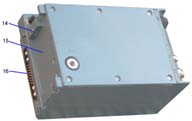
Receiver Synthesizer
The Receiver is the heart of the
FS5000 system. It contains not only the receiver but
also a digital synthesizer with a number of outputs and also
has the DB-25 connector that interfaces to the transmitter
controller.
The receiver covers 50 kHz to 30 MHz USB (which will receive
AM also) in 1 kHz steps. Uses either a 1 meter
telescoping whip screwed into the top of the receiver or an
external long wire connected to the antenna tuner -
Transmitter combination.
When the Receiver is mated to the Transmitter and turned on
the LED display shows 00000 with a decimal point on each digit
and the frequency change buttons have no effect.
The synthesizer provides:
- a fixed 50.0 Mhz LO to the modulator
- an LO that varies with the tuned frequency to the
modulator:
LO = Tuned Frequency + 50.2 MHz
- a 200 kHz clock for the digital modulator in the
Transmitter box
- a 75 Hz clock to pace the transmitter controller when
it's sending data to the transmitter
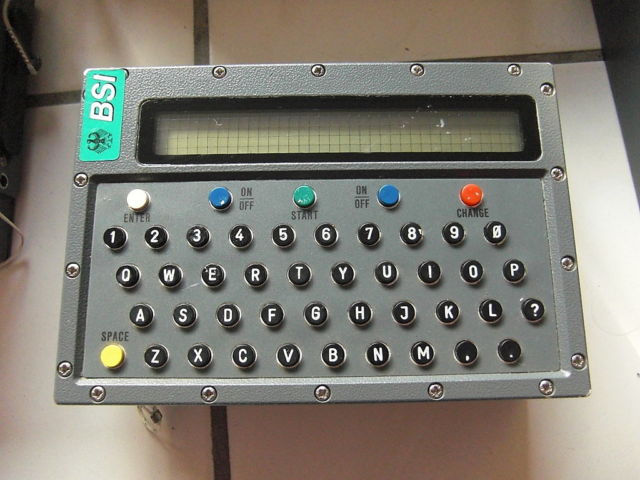
Controles & Indicators &
Connectors
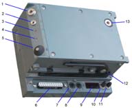 On a 45 degree sloping small panel,
left to right:
On a 45 degree sloping small panel,
left to right:
1 = <Delta>F - fine receive frequency control
2 = Headphone Jack
3 = + red LED
4 = - red LED
5 = Volume Control
On the top surface is a threaded hole (15) that would
accept the telescoping antenna.
A lower small panel has left to right:
6 = DB-25(f) connector, no coax porst - This is the interface
to the missing Transmitter Control Box
7 = F <- button for frequency digit select
8 = f ^ button to change frequency of one digit
9 = 5 digit LED frequency display (1 kHz to 29,999 kHz)
10 = 300 - 3000 toggle switch for IF bandwidth
11 = OFF - On toggle switch
Just above this panel (12) is the mechanical latch mechanism
to hold the Transmitter Controller.
On a side there's a DB-39 shell
(16) with 17 male pins and 4 female coax connectors.
This connector will mate to the one on the "H" 4 connector
block in the "S,X" packing box. The "H" bar is a way to
connect one battery to the Receiver for receive only
use. This connector also mates to one on the
Transmitter, but not to the other connector on the the
transmitter that appears to be similar, not becasue it's the
wrong connector, but because there are metal pins the prohibit
making that connection. This design seems fool proof.
The "2" metal plate can be placed on the Transmitter, prior to
attaching the Receiver, sitting in the groove with the hole
nearest the edge of the transmitter and with the lugs facing
the Receiver. Then, after the receiver connector is
mated to the Transmitter the plate can be moved toward the
batteries and it will "snap" into place by means of a plastic
part (14) on the back (15) of the receiver.
The two each "1" metal plates are for latching the batteries
to the transmitter.
The "3" metal plate is for latching the Transmitter controller
to the transmitter.
Receiver Connectors Wiring
DB-25 (6)
|
17 pin (Con 16)
|
Function
|
1
|
|
|
2
|
2
|
|
3
|
3
|
|
4
|
4
|
|
5
|
5
|
|
6
|
6
|
|
7
|
7
|
|
8
|
|
|
9
|
9
|
|
10
|
10
|
|
11
|
11
|
|
12
|
|
|
13
|
13
|
|
14
|
|
|
15
|
|
|
16
|
|
75
Hz sq wave out
|
17
|
|
digital
data out
|
18
|
12
|
|
19
|
|
|
20
|
|
|
21
|
|
|
22
|
|
|
23
|
15
|
|
24
|
16
|
+12
V in |
25
|
17
|
12
V return |
The reason there are a number of common pins may be
that these are "pass through" lines where the Receiver does
not do anything to these signals. There are 12 of these
signal lines.
DB-25 Power
By powering the Receiver using pins 24 (+14 V) and 25 (gnd)
the Tx interface connector can be probed with the receiver
active. The receive current draw is about 200 ma.
The A3 connector has a 200 kHz sine wave output with about 350
mv pk-pk amplitude.
The A2 connector has a 50 MHz sine wave that's probably around
350 mv pk-pk, measures about 150 mv on my HP 54501A 100 Mhz
scope.
Tx Interface Con 17 DC voltages in receive mode
Pin
|
VDC
|
1
|
0
|
2
|
0.28
|
3
|
0
|
4
|
0
|
5
|
0
|
6
|
0
|
7
|
5
|
8
|
0
|
9
|
0.94
|
10
|
0
|
11
|
0
|
12
|
0
|
13
|
0.45
|
14
|
0.94
|
15
|
0
|
16
|
13.98
|
17
|
0.0
|
Digital Data
Looking at the Rx DB-25 connector (6) pins with a scope shows
a 75 Hz square wave on pin 16 and digital data on pin 17.
Bottom Digital PCB
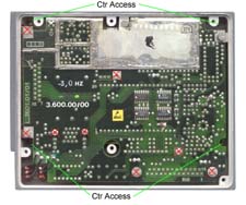
On the PCB in the bottom of the receiver
between pins 3 and 4 of the 4 coax connector (16) there are
small drops of black and green dielectric that appear to be
capacity tweaking. Just above this nest of traces is the
stamped message: "-3,0 Hz". These dots are some
type of revision marking, not tweaking. They appear on
many of the other boards in close proximity to the long white
silkscreen number that's the board ID, typically a group of 3
dots, probably using reisitor color code, so black black green
would be 005.
The PCB ID may be "L.3601.01/01" that's etched in metal
whereas "3.600.00/00" is printed in white paint.
The DB-25 connector is at the bottom right of the photo and is
labeled "BU2". In the center of the PCB there's what
appears to be a 38 pin IC and pins 1, 19, 20 and 38 are
numbered. The ICs: 4011 (2 input NAND), 4013 (Dual D
FF), 4023 (Triple 3 Input NAND) & 4093 (Quad 2 Input NAND)
are inside the 38 pin pattern.
Opening up the bottom Synthesizer
Screws Not to be removed
The two (-) scrwes holding the 4 coax support blocks
and the 4 (+) screws in the center of the PCB
and the two (-) screw sholding the DB-25 connector hex nuts
should NOT be removed when taking the PCB out of the
box.
Screws to remove
After removing the 2 (-) screws near the shield can,
the screw and 5 mm nut on the top of the DB-25
connector and pressing it down to free the Silicon sealing,
the two (+) screws holding the 4 coax connector to the box
can be removed.
The 4 (+) captive screws that release the bottom from the
top of the receiver. Seperate the top and bottom by
folding the two parts using the 4 coax cables as a
hinge. Then unplug the 4 coax connectors from the
bottom part. Note the 4 coax connectors have shrink
tubing labeled to match the call outs on the bottom shield
metal palate.
Now the PCB be lifted up on the edge furthermost away
from the 4 coax connector. The 4 coax connector is
holding the board now because of the Silicon
seal. The 4 coax connector comes out with the
PCB. I left the wires going to the bandwidth and
On-OFF toggle switches.
There's a big screw on top of the bottom synthesizer
housing, but it only holds a TO-5 heat sink which attaches
to a transistor by fingers, so it does not need to be
removed, the transistor just unplugs.
Bottom Synthesizer

There is a 10 MHz Tele Quarts OCXO marked
- 3 Hz.
A 44 pin metal can IC marked KS 1075 and a 38 pin metal can IC
marked KS1076.
Also a shield can has been constructed over a part of the PCB
that about 88 x 31 mm.
A 16 pin IC SP8690A (prescaler) , CA3140T, and what may be a
few op amps or transistors.
This is probably all synthesizer circuitry.
PCB is a 4 layer board, not a 3 layer as I previously
thought. This can be seen by looking at the area
adjacent to the DB-25 connector on both sides of the board.
Top RF &
Mixer PCB
The inside of the bottom cover
has a sheet of RFI gasketing with fingers that go all the way
around the cover to box joint. Maybe
TEMPEST level
shielding.
The top cover also has TEMPEST type
shielding. There are two compartments on the top
side.
The First is associated with the antenna and it has only a red
wire and a coax going to the other section. The PCB is
marked 3.100.00/00 in white paint. There's a SPDT switch
beside the antenna socket that's actuated when the telescoping
antenna is installed. Also near the antenna socket there's
a static snubber and some diodes maybe as signal level limiters.
The SPDT switch appears to be installed after a 3 transistor RF
amp. This is a very hot amp and you may get better
reception with the antenna not extended. There is one coax
coming into this compartment to a spot on the PCB marked "ST1"
which is not far from the SPDT switch. Most likely this is
the RF feed from the Transmitter when in receive mode.
There are 6 shielded inductors (L7, L8, L9, L10, L11 and L12)
which may indicate the frequency spectrum is broken down into 6
bands. Maybe:
Band 1 0.5 - 0.989
Band 2 0.989 - 1.957
Band 3 1.957 - 3.873
Band 4 3.873 - 7.663
Band 5 7.663 - 15.162
Band 6 15.162 - 30.0
This way each band is just under one octave wide, making for
good filtering and low spurs. But it would be difficult to
get good band separation with just the inductors in the front
end. Maybe they are just part of the filtering
scheme. There is another level or two in the receiver
between this board and the bottom board.
The other compartment on the top level looks like the LO and
mixer section. It's marked 3.200.00/00 in white paint.
There are 4 crystals fairly close to each other and centered in
the compartment. The frequencies are 50.191, 51.556 &
two others that can not easily be read. Interesting that
they are close together in frequency. There are some wire
gimmicks near the crystals and signs of tweaking with dielectric
paint. This probably is a crystal filter at the frist LO
frequency that's centered at 50.2 MHz.
Thre are a number of 0.1" type jumpers around the IF section:
12-13-16 may be between the RF and IF sections
3-4-5 is next to an RF/or IF transformer
2-14 is near another transformer
10-11-15 is near an IF can.
There are 2 coax cables going down from this compartment.
The one marked "17" goes to A2 on the 4 coax connector
(16). This is also the LO going to the transmitter
connector 20-A2.
The other coax has a connector marked "310" and the jack
on the PCB is marked "2" and it does not appear to be routed
outside the receiver box. Jack "2" is right next to a
BFT66 transistor marked "1". This might be the IF output
going to the rest of the receiver.
Local Oscillator
The top receiver PCB coax connection "17" seems to be a LO
comming from the synthysizer on the center level. This LO
signal also goes to the transmitter by way of the A2 coax
connection (16).
The LO is on the high side of the tuned frequency:
LO = Tuned Frequency + 50.2000000 MHz
The first IF is at 50.2 MHz.
Summary of the top PCB
The whip antenna always feeds a
3 transistor amplifier. Either the amplified whip RF or
the RF from the Antenna Coupler by way of the Transmitter is
selected by the switch in the whip antenna socket. The
RF then goes to one of the 6 single pole band pass filters
then via a 1" coax to the mixer compartment. After
mixing it's put through the first IF filter centered at 50.2
MHz and fed down the "310" coax to the central IF
boards. The LO (at the Rx frequency plus 50.2 MHz) is
also fed to the transmitter on the A2 coax connector.
Tx top PCB shows A1 as the variable LO
and A2 as a fixed LO freq. which seems different from A2 being
the variable LO port?
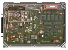
Central IF PCBs

After
the bottom cover is removed and the 4 captive screws down behind
the notches in the bottom PCB are backed out the receiver case can
be split open. Connecting the top and bottom portions of the
receiver are 4 coax cables and a miniature DB-15 pin connector
that may be identical to the one used for the
SVM-68 to radio connection. The coax
supplying the signal from the antenna tuner is marked 101 on the
bottom half of the receiver. The LO comes up from the bottom
through the 210 coax. It's not clear what the 311 and 411
coax cables are carrying.
There appear to be 2 PCBs in the top side. The deeper one
has a couple of mechanical filters on it marked:
FZ2410 (200 Pf, 130 pF) and FE 223 (39 pF, 39 pF) The
circuitry appears to be analog IF. There is a 24 pin chip
marked:
TEZ, C 18081 S, 103707, what is this?
The top most PCB is marked 3.400.000/00 with ink dots of 001.
The copper shield with the spring fingers on the bottom part is
marked 3.520 with color dots of 000.
There are no PCBs on the lower side, just a sheet copper shielding
material with fingers all around the perimeter.
15 Pin Miniature Connector between top
& Bottom of Receiver BU10
Note that this is the only non coax connection between the bottom
of the receiver (where the DB-25 Tx control connector is located
and the Top of the receiver containing the RF, IF and demodulator
are located.
Pin #
|
Name
|
Function
|
Tx
Interface Con
|
1
|
|
Digital
data from
receiver top
|
17
|
2
|
Tdc
|
+5v =
Tx DC on
T/R relay to T |
9
|
3
|
Gnd
|
Ground |
25
|
4
|
|
|
|
5
|
|
|
|
6
|
Gnd
|
Ground
|
|
7
|
TCL
|
T BU
1-6#4 TCL |
12
|
8
|
|
|
|
9
|
|
R 75 Hz
sq wave |
16
|
10
|
Gnd
|
Ground |
25
|
11
|
|
|
|
12
|
|
some
top receiver i.e.
RF, IF or demod related
|
14
|
13
|
Gnd
|
Ground
|
|
14
|
+12V
|
+ 12 V
to R |
24
|
15
|
|
|
|
There is also a flat in line10 pin connector ST2 that goes to the
boards above the PCb visable when the top and bottom parts are
parted.
BU1 is a 9 conductor buss connecting to the PCB directly below
that connects to the two IF filters. There is a resistor
between raised terminals 1 and 2 and another between terminals 6
and 7 that are factory select resistors that were installed after
the box was assembled.
BU9 and test point 13 are the coax going to 411 on the receiver
bottom.
Coax 311 on the bottom goes to the PCB holding the IF filters.
Encrypted Digital Transmit and Receive
There is no
indication that a microphone or key is used with this
system. There are some clues that indicate this is a
transceiver designed for sending and receiving encrypted digital
traffic.
The two LEDs on the receiver marked "+" and "-" and the associated
delta frequency screwdriver adjustment would be needed to get the
Receiver tuned correctly to some type of digital transmission.
The single low quality ear phone could be used to hear the data
and during the receiver tune process, but not for receiving a
message.
The DSU may be for combining a key and the data stream or maybe as
part of a test of the Transmitter Controller.
No micro controller in Receiver
There is no visible micro
controller (or microprocessor) in the receiver. The lower
section has the frequency synthesizer function. The
synthesizer PCB has two hermetically sealed can large pin count
custom ICs where the top IC is mounted to a daughter PCB that
sits directly over the lower 38 pin part. There are a
number of coax lines going from near the bottom chip and from
the daughter board to the shielded box at the rear of the
synthesizer PCB which must contain the VCO and related RF
circuitry. These parts provide the digital synthesizer
functionally. Although it's possible that they contain a
micro controller which might be used for other things, it's
extremely unlikely.
Note that the Antenna coupler does contain a micro controller
and it is in the form of 5 seperate large pin count micro
controller specific chips. Although it's possible for the
Antenna coupler micro controller to respond to commands sent by
means of the DB-25 connector on the receiver it's also very
unlikely. If the Antenna coupler micro controller was
running the rest of the system then the DB-25 connector would
properly be on that box instead of on the Receiver box.
The Antenna coupler does have the F0, F1, F2, F3 and FC lines
and so will know what frequency has been programmed into the
FS5000.
If this section is correct and the Receiver does not have any
intelligence then the command structure will be fairly simple
and close to what is done using manual frequency entry.
Transmitter Controller
April 2012 - systems on eBay Germany
with Controller, but I missed them.
Photos from eBay 2019 seller
sphany13
Warning
If you are going to be
working on making a controller you MUST fuse the hot and
ground wires to the DB-25 connector
and make absolutely sure
that none of the DB-25 wires can touch ground even for a
microsecond.
I let the smoke out of my receiver PCB and needed to make a
repair and someone else has had to go through the same pain.
When
the following modules are combined: Transmitter, Antenna coupler,
Mains power supply, battery Charger, Battery, Battery Receiver and
accessory Kit there is a space under the accessory Kit and in
front of the Mains power supply and charger and to the right of
the Receiver where the Transmitter Controller fits.
On the left of the Tx Ctrlr there is a downward pointing DB-25m
connector to mate with the connector on the receiver. Also
pointing to the left are a couple of pins with heads (similar to
pan head screws) that are captured by the lever on the Receiver
and as the lever is closed the pins are forced down which mates
the two DB-25 connectors. The Receiver has a 3.43 mm
diameter pin that goes into a hole on the transmitter controller.
There are no connections to the Mains supply or to the battery
Charger. This is logical since the FS5000 may be deployed in
the field without them.
Based on the
6 & 8 Dec 2004 email the
Transmitter controller would have the following functions:
Keyboard for data entry
Frequency input for Tx and Rx
Input of crypto key
Display for frequency or data
Clock to transmit automatically so agent wuld not need to be
there
Lithium battery backed retention of received messages to
allow NiCad batteries to go flat without loss of Rx msg
This is missing from the systems that have been sold as
surplus. It probably fits in one of the small boxes.
The space under the accessory kit suggests that the size is 45 mm
high, 125 mm wide (150 mm including a DB-25m connector) and 100 mm
deep
The controller has a DB-25m connector that mates to the Receiver's
DB-25f connector (6) and is machannically attached to the system
using the lever (12) on the Receiver. Note this lever is
designed to press the Transmitter Controller down onto the
Receiver's DB-25 connector (6).
10 Aug 2006 - Some speculation about the controller. It
probably contained some type of encryption/decryption that was not
a one type pad, but rather more like DES where a key is used
that's much shorter than the message length. The Transmitter
and Receiver were probably controlled by a timer in the control
box. That way the spy would not be near the hardware during
either transmission or reception. The crypto key would work
in such a way that the data to be sent would be encrypted and the
key erased prior to placing the transmitter. When receiving
a message the encrypted message would be stored in the controller
and only later when the key was entered could the plain text
message be seen.
HFS7000 Radio and TCU7000 Control Box
The HFS 7000 military radio made
by Telefunken has specs very similar to the FS5000. More
interesting is the TCU7000 control box. At the top it has
a 2 line by 40 character LCD. Directly under the LCD and
evenly spaced are 5 keys marked F1, F2, F3, F4 and F5 that
relate to legends displayed directly above them on the lower
line of the LCD, i.e. a menu system.
The Telefunken HRM 7000 is very similar,
Manpack,
Vehicle
&
Fixed
versions.
Brochure
for 7000 Family.
Below the function keys there is a 4 row typewriter style
keyboard with 41 keys. To the left of "A" is what's
probably the shift key. At the right of the row starting
ASDF... is a larger key that's orange in color. This might
be used with the shift key as a zeroize key.
F1
F2 F3
F4 F5
1 2 3 4
5 6 7 8
9 0
Q
W E R T
Y U I O P
^
A S D F
G H J K L
<Orange key>
Z
X C V B
N M ; . -
DB-25 Transmitter Controller Interface
Connector (marked # 6 in Receiver photo)
Tx
Controller
Rx con 6
|
Rx con 16
Tx con 20
|
Tx con 17
Ant Cplr con 24
|
DB15
|
Name
|
Function
|
RBH
VDC
|
TRBB
(no A)
V DC
|
TARBB
V DC
|
1
|
|
|
|
IFBW
|
open=3kHz,
gnd=300
Hz
Note 6
|
4.66
|
0.50
|
0.5
|
2 RA
|
2
|
3
|
|
F0
|
A F0 Note 11
|
0
|
0
|
0.2
|
3 RA
|
3
|
2
|
|
F1
|
A F1
|
0
|
0.4
|
0
|
4 RA
|
4
|
7
|
|
F2
|
A F2
|
0
|
0
|
0
|
5 RA
|
5
|
1
|
|
F3
|
A F3
|
0
|
0
|
0
|
6 RA
|
6
|
9
|
|
FC
|
A FC Note 10
|
0
|
0
|
0
|
7 RA
|
7
|
|
|
Fman
|
/Rcvr Man
Freq Lock Note 2
|
5
|
5
|
0.9
|
8 r
|
|
|
|
RxOff
|
open=Rx
on, gnd=Rx Off
Note 5
|
5.2
|
5.1
|
5.1
|
9 T
|
9
|
|
2
|
Tdc
|
+5v =
Tx DC on
T/R relay to T
Must be off for Rx
|
1.9
|
0.3
|
0.3
|
10 T
|
10
|
|
|
TX
|
T BU
1-6#1 TX
|
0
|
0
|
0
|
11 T
|
11
|
|
|
RF
|
T BU
1-6#2 RF
+5v = RF on
|
0
|
0
|
0
|
12 TR
|
|
|
7
coax
|
TCL
T0
|
T BU
1-6#4 T0
connects mod exciter directly to ATU
for preliminary ant tune
no connection to synth
only top RF, IF
Note 9
|
0
|
0
|
0
|
13 TR
|
13
|
|
|
SL/Tune
|
0.8 =
Synth lock
hi= no lock (floating?)
Note 7
|
0
|
0
|
0
|
14 R
|
|
|
12
coax
|
AGC
|
Gnd =
full gain
high = no gian
Note 8
|
1.2
|
0.8
|
0.8
|
15
|
-
|
-
|
-
|
-
|
no
connection |
0
|
-
|
-
|
16 RT
|
|
|
9
|
CLK
|
R 75 Hz
sq wave out
Note 3
|
2.5
|
2.5
|
2.5
|
17 RT
|
|
|
1
|
RxD
|
R digital
data out
Note 1
|
jumping |
jumping
|
jumping
|
18 T
|
12
|
|
|
?
|
|
0
|
0
|
0
|
19
|
|
|
|
?
|
|
0
|
0
|
0
|
20
|
-
|
-
|
-
|
-
|
no
connection
|
0
|
-
|
-
|
21
|
-
|
-
|
-
|
-
|
no
connection |
0
|
-
|
-
|
22
|
-
|
-
|
-
|
-
|
no
connection |
0
|
-
|
-
|
23
|
15
|
|
|
?
|
|
0
|
0
|
0
|
24 R
|
16
|
|
|
+12V
|
+ 12 to R
Note 4
|
14.98
|
14.58
batt
|
14.58
|
25 RT
|
17
|
4
|
3, 6
10,13
|
Gnd
|
Ground
|
0
|
0.0
|
0.0
|
A capital letter appearing in the
Pin column means there is a connection to that box, a small letter
means the connection has a resistance greater than 1 Meg
Ohm. All measurements made with no batteries or power
connected.
Note 1 - Digital TTL data from the
receiver demodulator.
13 Dec 2004 - This data switches from about -0.060 Volts to +5.06
volts and is coming from the demodulator in the receiver.
That's why sometimes it's there and other times it's not.
By sending in a 20.000000 MHz signal with a 100% AM square wave
modulation at 420 Hz the output is not a square wave but quite a
few pulses with flat tops. With the delta frequency control
set fully CCW the output is about 0 volts and when fully clockwise
mostly +5 volts.
Phase modulation also causes the TTL digital data.
Adjusting the fine frequency control with a small screw driver
will cause the data to come and go. This indicates that the
receiver really should be able to tune in 0.1 kHz steps and not
the existing 1.0 kHz steps. I have not found any combination
of RF frequency, FM deviation and modulation frequency that will
cause a digital output.
This means that the transmitter controller would need to take in
this TTL serial data stream and convert it into a message.
This probably included applying some cryptographic cipher.
Note 2 - The actual function of pin 7
is not yet known.
The
email of 6 Dec 2004 indicates that
the Tx and Rx frequencies can be split (set to different
values). This would require a way to tell the FS5000 that
the following frequency input was either for the transmitter or
receiver. Pin 7 effects the input of frequency data and is
adjacent to pins 2, 3, 4, 5 and 6 which I think are used for
remote frequency entry. This proximity in the pin numbering
is a strong indicator that this pin is also related to frequency
entry.
9 Dec 2004 - When 4.5 Volts is applied to this pin in the TARBBMC
configuration the setting of a frequency is enabled. Without
this pin high you can not change the frequency in the TARBB or
TARBBMC configurations. Also if the main ON-OFF switch is
turned off and later back on all the digits to the left are still
there, but the right most digit is a zero with the decimal point
indicating that it should be set. If the power switch is
cycled the decimal point moves to the left and the next digit is
now zero.
Note that when the Antenna coupler is attached to the system it
pulls this pin low turing off the ability to manually set the
receiver frequency. Connecting just the transmitter does not
effect this pin.
Note 3 - This square wave could be used
to drive a clock in the Tx Controller. Seems strange that
it's not 60 or 50, but it would be no problem to divide it by 75
to get a one second tick. The advantage would be that the
oscillator in the Receiver is a very high quality unit and so
would allow keeping very good time. The problem is that when
the main batteries go dead the clock would stop. This may or
may not be a problem.
If the Transmitter Controller had an independent clock then it
could turn the FS5000 on and off a number of times on some
schedule of repeated attempts to both receive messages and to send
a message. This could be done over and over where in the end
the attempts were no longer effective since both of the batteries
have gone dead. This type of approach would be good for
getting a message through but not so good in terms of minimizing
the talk time and hence the ability of the local DF unit to detect
and locate the FS5000.
13 Dec 2004 - After seeing that
pin 16 is the demodulated digital data output checking pin 16
shows a 75 Hz square wave with magnitude -0.06 to +5.06
Volts. Testing in the RBH configuration. Turning off
the RF has no effect on the 75 Hz clock that comes from the
synthesizer, not the RF-IF-audio part of the receiver.
14 Dec 2004 - This may be a clock used to synchronize data bits to
be transmitted with the modulator. This clock is probably
locked to the 200 kHz clock that drives the modulator. Since
at every change on the TX pin causes some number of cycles of the
modulator it's important that the modulator be driven
synchronously. For testing this signal might be feed into
the TX pin?
Note
4 - the battery voltage that is on pin 24 is for powering
the transmitter controller and not for powering the receiver for
normal use, although it could be used for receiver testing.
Note
This is
extreamly dangerous.
If
shorted it will smoke the bottom Receiver PCB!
Note
5 - If pin 8 is pulled to ground the receiver turns
off. If pin 8 is then floated the receiver stays off.
When pin 8 is pulled up the receiver turns back on. It's
probable that the transmitter controller has a pull down resistor on
pin 8 so that when it's connected to the FS5000 system the system is
normally off. Pin 8 is then pulled high to turn on the
receiver. The power for this can come from the DB-25 connector
pin 24 and/or from the battery that's internal to the Tx
controller. Test done in RBH configuration.
Note 6 - The receiver IF bandwidth switches to 300
Hz when pin 1 is grounded and goes back to 3,000 Hz when the pin is
floated. Test done in RBH configuration.
When the transmitter is connected to the receiver this pin is pulled
down automatically switching to the narrower bandwidth.
Some speculation on why the 2 receive IF bandwidths. The
transmit modulator has a 500 Hz output center frequency and probably
has a bandwidth less than 300 Hz. When initially tuning in a
station the 3,000 Hz position is used then after the station is
centered using the fine adjustment the BW is switched to 300 Hz to
improve the s/n ratio. If only one remote station is being
worked the fine frequency adjustment may need to be made once and
from then on it should be good for any frequency transmitted.
Note that selecting the narrow bandwidth also turns off the LED
display, that's why connecting the transmitter to the receiver
causes the LED to go black.
Note
7 - For receive operation when a pull up resistor is
applied to pin 13 and the synthesizer is not locked the pin is
pulled to ground. When the synthesizer is locked then the pin
is open and can be pulled up to 5 Volts.
For transmit operation, after a frequency has been set into the
synthesizer, while the antenna coupler is tuning the line stays low
(meaning correct frequency), but when there's a successful antenna
tune the line goes high.
Note
8 AGC - This is the AGC line and can be used two ways:
Looking at the voltage on
this line gives an indication of the signal strength.
1 Volt for noise
3 Volts for a strong signal
The AGC can be pulled up or down:
Pulling down increases the gain
Pulling up lowers the gain
Blown PCB traces & Repair
22 Nov 2004 - Found open trace from pin 25 and repaired
it. When turned on in configuration RHB noticed that the
Red wire from pin 24 had exposed conductor and started to get
some tape to cover it, but it touched the black wire causing
smoke. So now I know why the pin 25 trace was blown
open. But my repair made this trace have higher current
carrying capability. Now a trace that's in the center of
this 4 layer board has blown. It will be more
difficult to repair it.
8 Dec 2004 - By soldering a #30 wire wrap wire from the DB-25
pin 24 to the Tx interface connector pin 16 the Receiver has
been restored to working condition.
In the RTBBX configuration when
Tdc
is pulled high a pulse train appears on pin 17. -4 V to + 1
V at a frequency of 1.25 kHz. High for 400 uS and low for
100 uS. In the RHB configuration this does not happen.
Note 10 -FC (21 Nov 2004)
When in the RHB (Receiver, H bar & Battery) configuration and
the LED display is on, the FC pin has a clock signal at about 500 Hz
with voltage levels of +100 mv and - 50 mv. I would call this
a weak and noisy signal, not one that's useable.
If the LED is turned on and one of the inner digits has the active
decimal point and then a pulse is applied to the FC line the active
digit moves to the left just as if the "<-f" button was
pressed. So it looks like this is the Frequency Column input.
Note 11 - F0, F1, F2 & F3
There are not enough unaccounted for
pins for the transmitter controller to use pins (i.e. parallel
data) to set the transmit frequency so it's probably done with a
serial data stream or using the frequency butttons on the
receiver. The F0, F1, F2 and F3 signals might be the high
order frequency bits. 2 ^ 15 is 32768 so it would take 15
bits to specify the frequency to 1 kHz. The bit
weights would be: 1, 2, 4, 8, 16, 32, 64, 128, 256, 512, 1024,
2048, 4096, 8092 and 16184 kHz. Then the meaning of the F0
through F3 bits might be: 0, 2, 4, 6, 8, 10, 12, 14, 16, 18, 20,
22, 24, 26, 28, 30 MHz
If BCD weighting was used then the 10 MHz digit would need 2 bits
and the other 5 digits would use 4 bits each for a total of 22
bits. Then the F0 and F1 might be associated with 10 MHz
(i.e. 0, 10, or 20 MHz would be valid) and the F2 and F3 would be
the 8 and 4 MHz bits for the 1 MHz digit (i.e. 0, 4 or 8
MHz). If this was the case the the possible meanings
would be: 0, 4, 8, 10, 14, 18, 20, 24, 28, 30 MHz. There are
9 small green LEDs next to the transmitter output filter bank so
this may be more likley than a pure binary bit assignment.
The Transmitter needs to know how to select the correct output
filter and the antenna tuner needs to know roughly the frequency
that needs to be matched (this determines which matching elements
are significant and which don't matter). This can be provided by
the 4 Band select bits.
20 Nov 2004 - New Theory
The receiver can be manually tuned
using just two momentary push buttons, one to change the
Frequency column and the other to advance the selected frequency
digit. One way to do this would be to have parallel switch
contacts on the DB-25 connector. Maybe Frequency Advance and Frequency Column wires? Another
way that would be faster is to have a nibble (1/2 of an 8 bit
"bite" i.e. 4 bits is called a "nibble") to set the frequency
digit and that takes 4 wires (F3, F2, F1, F0) and still needs
the Frequency Column function, but no longer needs the Frequency
Advance function. This would allow setting any frequency
very quickly, supporting either hopping or a sweep.
Testing this is the next order of business.
The FC line has the
same effect as the "<-f" button. This means the new
theory may very well be how the controller sets the frequency.
21 March 2005 - Remote Rx Freq Procedure
Ray
Robinson has discovered the key to remote programming the
receive frequency. This must have been difficult since the
LED frequency is blanked during remote frequency entry. It
turns out that the controller sets 7 digits of frequency like
12,345,670 Hz. where the 1 Hz digit can not be set but the 10 Hz
and higher digits are set. This makes sense since setting
to 10 Hz is about the same as using the manual fine tune knob.
Note that the LED display has only 5 digits (i.e. down to 1
kHz), but using the controller you might be able to set with 10
Hz resolution, although it's not clear if the least significant
digits really are setting the frequency.
The procedure is:
- go into Rx mode by setting RxOff high
- Set IF BW to narrow by setting IFBW to ground or leave it wide by setting IFBW hi or open.
- Set Fman high
(when high it's Fremote)
- <label loop> use F3, F2, F1 & F0 to set the
frequency starting with the 10 Hz digit using BCD weighting
(F3=8, F2=4, F1=2 and F0=1).
- Pulse FC high to
latch the frequency & move one column to the left
- <go to loop to set all 7 digits>
- set Fman low
Ray's
Basic
program to drive the printer port on a old PC needs an
adapter board in line between the computer and the FS5000.
Note that Ray also
suffered
bad luck by allowing part of the
adapter
board to short out the power line and smoked part of his
receiver bottom PCB.
So the recommended hookup is as follows:
[computer] [Centronics-----cable----DB-25f] [DB-25m---adapter
board---DB-25f] [DB-25m----cable----DB-25f] [FS5000]
This way the connection at the FS5000 is clean with no chance of
a problem there, but the
adapter
board
is still critical.
28 March 2005 - Tx with Ant Coupler
Procedure (no Modulation)
This procedure activates the transmitter after the antenna
coupler has tuned the antenna.
- Set Rxoff high
- Set Tdc high
- Set Fman high
- For I = 1 to 7
- Set BCD frequency digit
- Pulse Fc
- Next I
- Set Fman Low (now F0, F1 & F2 are the LPF select
lines)
- Set LPF (0 through 7 on F0, F1 & F2)
- Wait for Synth Lock to go high indicating good antenna
tune
- SET RF high to transmit
Transmitter Low Pass Filter
The LPF is set using the F0, F1
& F2 lines (F3 does not seem to have any meaning for
this). When Fman is low these lines select the LPF.
F2,F1,F0
|
LPF
|
0
|
Out
30 Mhz or 50 Ohms?
|
1
|
3
Mhz
|
2
|
4
MHz
|
3
|
6
MHz
|
4
|
8
MHz
|
5
|
12
Mhz
|
6
|
16
MHz
|
7
|
20
Mhz
|
-
Ray's
Basic language program now allows setting the Rx and Tx
frequency and switching back and forth between Tx and Rx
modes. It also forces a the antenna coupler to tune when
the Tx frequency is set. But the transmitter is only being
keyed on and off, no modulation is being sent or
received. The same
adapter
board is needed. There is a possibility that the
receiver is still operational during transmit, so the radio may
have full duplex capability. The Function keys on the PC
keyboard are:
- T = switch to transmit mode without changing the antenna
tuner
- R = switch to receive mode
- 8 = Input a 7 digit receive frequency Example 1400000 is
14 Mhz)
- 9 = Input a 7 digit transmit frequency (-200 kHz offset
applied by synth) Example 1380000 is 14 Mhz & force
antenna tune
- X = eXit program
Note there is no fuse in the receiver box so if pin 24
is allowed to touch ground (pin 25 or any metal on the
FS5000) traces on the receiver PCB will be destroyed and a
repair will be needed. See the 21
March 2005 post for a suggested cabling scheme that
will minimize the danger.
4 April 2005 - The
controller lines should be shielded both to prevent computer
generated hash from getting into the FS5000 and also to keep the
FS5000 output RF from getting into the computer.
22 April 2005 - A note
on the offsets needed for using the FS5000 for CW ops to work
with the USB Rx mode of the FS5000.
- Tx freq 200kHz lower than the actual transmitted signal
- Rx freq 1 kHz lower than the operating freq.
Procedure to Turn on Transmitter
- First you have to disconnect the purple-white wire that
connects to the Tx 17 pin connector, from inside the Tx
unit. This will enable the Rx controls to operate while
connected to the Tx. This is not necessary if the
Antenna Coupler is not installed.
- Then by applying a TTL +5v signal to pin 9 (Tdc)of the DB-25
connector, the Tx unit will turn on. This also
disconnects the antenna to the Rx. Green LED's will
light in the Tx unit.
- By applying a TTL +5v signal to pin 11 of the DB-25
connector (RF), the
transmitter will key up, & transmit a signal.
Interestingly though, the Tx signal is exactly 200 KHz higher
than the Rx freq.
- Note that the Antenna Tuning unit is not active at this
point so you should have it disconnected from the transmitter
and take the transmitter output directly to a matched antenna
or the Transmitter test X Box. The frequency set into
the receiver needs to be 200 kHz below the desired transmitter
QPSK output frequency.
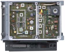
Controler Chassis
Transmitter
 This
transmitter uses digital In phase and Quadrature ( I&Q)
modulation methods which are very much more sophisticated than the
more common RTTY modes used on H.F. The mode is likley
either QPSK (Quadrature Phase Shift Keying) or OQPSK (Offset -QPSK,
where no 180 degree changes are made). The power output can be
adjusted using the "PO" pot near the final amplifier stage on the
bottom PCB. With the factory setting the CW output is about 40
Watts.
This
transmitter uses digital In phase and Quadrature ( I&Q)
modulation methods which are very much more sophisticated than the
more common RTTY modes used on H.F. The mode is likley
either QPSK (Quadrature Phase Shift Keying) or OQPSK (Offset -QPSK,
where no 180 degree changes are made). The power output can be
adjusted using the "PO" pot near the final amplifier stage on the
bottom PCB. With the factory setting the CW output is about 40
Watts.
The Transmitter interfaces to the Receiver and to both batteries or
to the Charger + AC Mains supply. The top 3 coax DB type
connector (17) mates to either the X Box or the Antenna Auto
Tuner. The A2 coax is the RF output that feeds the X Box for
Tx testing or feeds the Antenna coupler.
The front side has connectors for battery one (18), battery two (19)
and the Receiver D type connector with 4 coax ports
(20). On the side is a connector (21) that looks very similar
to the one used for the receiver, except this connector does not
have any coax connections instead the coax psitions are filled with
sleeves that prevent the receiver from mating. There's also
pins that prevent the receiver from mating. None of the pins
on connector (21) connect to other (21) pins.
There is a groove (22) above the three connectors (18, 19 & 20)
that holds the "1" (battery) and "2" metal locking plates.
Above the Tansmitter Controller connector (21) there is a groove
(23) to hold the "3" metal locking plate. There are also
grooves in the Antenna Auto Tuner just above the grooves (22, 23) on
the transmitter.
The only pins that are common between the two large connectors are
15 and 17 (gorund).
Tx Top PCB Modulation & LO Mixing
 One
side has a number of ICs. These include a couple of 28L22
PROMs wiich are arranged as 256 bytes and next to these are a couple
of AD7524 8 bit ADCs. They are not fast enough for RF
synthysis, but would be great for an I-Q modulator. Next to
these is a SE5514N Quad comparator and from this there is a PCB top
trace labeled SIN COS that ends near the MCL TSC-2-1 two way
splitter and a couple of TSM-1 mixers. This is for sure an I
& Q modulator. These are fed from the fixed 50.0 MHz LO
and the 50 - 80 MHz variable LO after amplification with the Avantek
amps.
One
side has a number of ICs. These include a couple of 28L22
PROMs wiich are arranged as 256 bytes and next to these are a couple
of AD7524 8 bit ADCs. They are not fast enough for RF
synthysis, but would be great for an I-Q modulator. Next to
these is a SE5514N Quad comparator and from this there is a PCB top
trace labeled SIN COS that ends near the MCL TSC-2-1 two way
splitter and a couple of TSM-1 mixers. This is for sure an I
& Q modulator. These are fed from the fixed 50.0 MHz LO
and the 50 - 80 MHz variable LO after amplification with the Avantek
amps.
The ICs that feed the PROMs are: UA139 (Quad Volt conp), MC54HC390
(Dual 4 stage binary ripple counter), MC14070B (Quad 2-input EXOR),
MC14015B, CD4013 (Dual D FlipFlop) and MC14093(Q. Next to this
last IC is a 6 pin header marked:
BU 1-6 Buss on both Transmitter boards and
elsewhere
Pin
|
Name
|
Function
|
1
|
TX |
Probably
the Data Input
|
2
|
RF
|
Turns on
Modulation
& ...
|
3
|
9V
|
Powers
Mod PCB
|
4
|
T0
|
Output
from Mod PCB
from PROM A4 address line
maybe a bit clock output
|
5
|
Tu
|
|
6
|
Gnd
|
Ground
|
The bottom PCB calls this BU 1-6. This seems to be the extent
of the non coax connections to this board.
RF
When RF is active the counters and
shift registers are allowed to count. When inactive they
are locked in reset mode. 47k pull down resistor.
The RF line drives a couple of 4093 NAND gates in series and
then drives the reset pins on the 4013, 4015 and 54HC390.
These are the counters that drive the PROMs which in turn drive
the A/Ds that do the SIN & COS modulation. They are
only counting when RF is high and reset otherwise.
Modulation will only be present when RF is active.
Note that RF does NOT
turn the Transmitter RF off. Tdc must be used for that.
T0 aka TCL
Is a 1 kHz output clock with a 1 k
Ohm source resistance from 4093 NAND pin 10 on the modulator
PCB.
This is the same as pin 12 (TCL) on the Transmitter Controller DB-25
connector. This is strange since the function of TCL is to
bypass the Transmitter Power Amp and send the low power
modulator output signal directly to the Antenna Tuner.
Note that the 1 kHz clock does not appear when the RF line is
inactive. It may be that the there are other logic states
that keep the 1 kHz turned off, like during antenna tuning and
the clock only appears when data is being sent.
This signal is not always connecteed the the Tx control DB-25
connector pin 12.
When in the RTBBX configuration DB-25 pin 12 has noise, but when
Tdc is pulled high the noise goes away and the voltage goes to
zero.
TX
Changes one PROMs A7 line, but NOT
the other PROM. This could be for one of two different
reasons (ony one of which is correct):
(1) when not TX then use a different PROM data pattern (i.e. a
possible tune mode)
(2) when TX send a "1" and when not TX send a "0" (i.e. TX is
the data input).
Tu
Most likley the Tune line. It
is neither a pure input nor a pure output, but rather a buss
line. It ends up controlling an input (pin 9) to the UA139
comparator. The other input to this gate (pin 8) is from
the 200 kHz input. The U6 comparator also has another gate
input (pin 10) that gets the 200 kHz input signal at the same
level as pin 8 but the other input seems to be from a fixed DC
level. The two comparator outputs from the UA139 are feed
into (pins 1 & 2) one of the gates of the 4070 XOR and the
output (pin 3) feeds the clock input of the 54HC390 counter that
drives the A0 through A4 address inputs of both PROMs. The
circuit surrounding the UA139 only has the Tu input (the only
place Tu is used on the mod PCB), the two identical 200 kHz
inputs and the two comparator outputs driving the XOR
gate. There are no other outputs from the UA139.
This rules out the use of modulation on the 200 kHz input as the
data signal since with the stock setting (2a=2b)of ST7 the 200
kHz goes nowhere else.
3 +9V - feed from the S200C adj. Voltage Reg that's next to
the BYS28-15 Dual Diode. This is the power to the modulation
Top Tx PCB.
There are 5 coax cables connected to this PCB:
ST3 input 50M goes to 20-A2 . (Fixed freq from Rx to mix with
variable LO to get Tx freq)
ST6 input 52..80 M goes to 20-A1 (variable LO from Rx
that's 50.2 MHz above Rx frequency, i.e. in the 50 to 80 MHz range)
ST4 output 2...30M, RUECKM. this goes to the 17-A3 coax in the 3
coax connector that mates with the Antenna Coupler.
ST5 output 2...30M MOD. goes to P/IN on the bottom PCB (RFm)
The actual low power signal to be transmitted.
ST2 200 KHZ this cable ends near the UA139, all the other cables are
on the analog side of this PCB. This is a mystery
signal.
Today (3 Nov '04) I think it's a
clock for the modulation circuits. The idea would be this
200 KHz clock drives a counter that in turn drives the 28L22 PROMs
address lines which are identical and contain a table that can be
addressed to provide either a SIN or COS function depending on how
they are addressed. 200 kHz divided by 256 is 781.250 Hz
which is an audio frequency.
There's a single crystal "12KV688, XF-500" that seems to be part of
a band pass filter with transformers on either side for
matching. Most of the filters in the FS5000 have 0.1" spacing
headers at the input and output, probably to allow tuning the filter
independently of the circuitry on the board. This may be a 500
Hz wide pass band filter.
There are 4 Mini Circuits Labs mixers on this board, a MCL power
splitter, and 8 Avantk unit amplifiers (GPD-120 and GPD-130).
The LM209H is a TO-5 packaged +5 Volt regulator that takes in the +9
from the BU 1-6 buss and powers most of the 40xx series ICs.
Tx Bottom PCB RF Amp & Output Filter
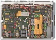 The RF
power amp consists of an MRF134 (about 3 Watts out) driving a small
transformer then an ON4347 driving a larger transformer then a coax
marked ST15 going to the center of a filter bank using 9 each DPDT
relays 16 inductors and 48 caps. There's also what may
be a high VSWR detector. Beside the filter bank there a string
of 9 small green LEDs.
The RF
power amp consists of an MRF134 (about 3 Watts out) driving a small
transformer then an ON4347 driving a larger transformer then a coax
marked ST15 going to the center of a filter bank using 9 each DPDT
relays 16 inductors and 48 caps. There's also what may
be a high VSWR detector. Beside the filter bank there a string
of 9 small green LEDs.
The BYS28-45 is a Dual Schottky diode where the center pin is a
common cathode. Although the large diameter wires appear
connected to this part, only the large orange wire is directly
connected. The others probably are routed thorugh the gray
ST1-DC12V relay with contacts rated for 5 AMps @ 30 VDC. This
is probably the Tx on-off control relay. All of the relays hve
12 Volt coils.
With the Antenna coupler mated to the Transmitter and no DC power
applied the DC resistance between the Red Antenna jack (26) on the
Antenna Coupler and the A4 coax on the Receiver interface connector
(20) is under 1 Ohm. So when the Transmitter is turned off by
the gray relay the combined Transmitter and Antenna Coupler just
directly connect the long wire antenna to the receiver.
The 4 coax cables leaving this PCB are:
ASG output cable marked ASG goes to connector 17-A2 mates with
Antenna Coupler or with X Box coax probably the RF output (ASG is
German for Antenna Tuner Unit)
RFTU cable marked P/TU goes to 17-A1 to/from Antenna
Coupler
RFM cable marked P/IN goes to ST5 on the to PCB (2...30M,
MOD.)
EMP input cable marked EMPF - goes to connector 20-A4
"Emp" stands for Empfanger which means receiver
There are a couple of SG203J ICs containing 7 relay driver
Darlingtons. Inputs are pins 1 to 7 with corresponding outputs
on pins 16 through 10 with pin 9 being the common of 7 clamping
diodes from each output pin. Each output is good for 500 ma of
relay current. The nearby MC14011B Quad 2 input NAND is
probably part of the logic decoding for the relay drivers.
There are also 4 small green LEDs near by that may indicate the
relay channel status. One of the 2003 chips is next to the
output filter bank (there's a string of 9 small green LEDs nearby)
and the other is near where the P/IN and P/TU coax cables terminate.
The CD4028BF is a 4 line to 10 line BCD to decimal decoder that's
driving the 2003. Where are the control signals coming from?
Transmitter Control Connector (20) 4 Coax +
17 pins
Pin
|
Function
|
BU 1-6
|
Antenna
Coupler
|
A1
|
50 - 80 MHz LO from Rx
|
|
|
A2
|
50.0 MHz LO from Rx
|
|
|
A3
|
200 kHz Clock from Rx
|
|
|
A4
|
Long wire ant to Rx
used when whip not installed
|
|
|
1
|
Ground
|
|
4
|
2
|
|
|
3
|
3
|
|
|
2
|
4
|
|
|
7
|
5
|
|
|
1
|
6
|
|
|
9
|
7
|
|
|
|
8
|
|
|
|
9
|
|
|
|
10
|
|
1 = TX
|
|
11
|
|
2 = RF
|
|
12
|
|
4 = TCL
|
|
13
|
|
|
|
14
|
|
|
|
15
|
|
|
|
16
|
+ 12 to Receiver
|
|
|
17
|
Ground
|
|
|
Transmitter DC Power Connector (21)
Note that while this connector looks
similar to the Tx Control Connector, the A1 through A4 positions
are filled with DC contacts, not coax contacts. It can be
used to power the Transmitter from the Battery Charger + AC Mains
power supply, or from a couple of batteries using the H Bar.
Why are there two ways to use battery power? Maybe to allow
continuos operation while batteries are changed? This is no
mistake, the two battery positions on the H Bar can only be used
this way.
Pin
|
Function
|
A1
|
DC Ground
side battery (18) thermistor
|
A2
|
nc
|
A3
|
heavy
brown wire
Battery charging?
|
A4
|
+14.0 V
from Batt Chgr |
1
|
|
2
|
center
battery (19) thermistor
|
3
|
Battery 2
+
|
4
|
|
5
|
|
6
|
|
7
|
|
8
|
side
Battery (18) thermistor
|
9
|
center
battery (19) thermistor
|
10
|
|
11
|
|
12
|
|
13
|
|
14
|
|
15
|
|
16
|
Battery 1
+
|
17
|
Battery 1
& 2 -
|
The thermistor connections indicate that the batteries can be
charged while the system is in the TCAMR23 AC
Mains powered Receive - Transmit configuration.
18 Nov 2004 - Scope Testing Tx while powered
Configuration MCRTX with top cover
removed. Breakout of Transmitter Control connector pins.
Using 3 ea. AA bateries in series with 1 k Ohm as source for Tx
Ctrl input.
+4.5 to
Tdc causes a
relay to click and BU 1-6 looks like:
Tx Ctrl
|
Pin:
|
1 T
|
2 RF
|
3 9v
|
4 T0
|
5 Tu
|
| Tdc = +4.14 |
Vdc:
|
0.01
|
0.002
|
9.08
|
5.02
|
13.91
|
Tdc = +4.14
RF = +4.14 |
|
0.003
|
3.44 |
9.11
|
note 1
|
14.06
|
note 1 - T0 is a pulse waveform. 0 to +5 volts, period of
500 uS, high for 400 uS and low for 100 uS, frequency 2 kHz
A0 = 20 kHz sq wave
AD7524 D/A pin Rfb is 500 Hz sinewave
ST10 = 50 MHz sine wave
stopped testing - X Box is hot
19 Nov 2004 - Spectrum Analyzer Tx
The crystal filter between ST11
(input) and ST12 (output) uses a single series crystal (single
pole) centered at 50.000 MHz. The 50.0 MHz signal that comes
into the modulator board at ST3 is amplified and I & Q mixed
with a 500 Hz data signal from the digital modulator and the
modulated 50.0 MHz signal is passes through the crystal filter to
get rid of some sidebands. It's then mixed with the variable
LO signal )Rx freq + 50.20 MHz) to produce a final frequency of Rx
+ 200 kHz. This signal is filtered and then amplified then
comes out ST5.
There is another signal path where the amplified but un modulated
input 50.0 Mhz signal gets mixed with the Variable LO to produce
the same output frequency as above and this signal is sent to ST4
called RUECKM and is used by the Antenna coupler.
Looking at the 500 Hz sin signal at ST8 with Tdc and RF pulled
high and briefly pulling TX high casuses the spectrm to widen for
a short time then look normal, so by using "data hold" on the
spectrum analyzer and stroking the TX line with +5 V the SA
captures the widened signal centered at 500 Hz. So TX is the
data input line and it needs to be changed to cause the spreading.
With Tx control lines Tdc and RF pulled high the BU 1-6 buss T0
line has a 2 kHz signal, but NOT pin 12 on Tx DB-245 control
connector, so the ohmic path that's there with power off is not
there when Tdc and Rf are activated.
Antenna Auto Coupler
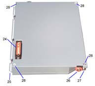 The
Antenna Auto Coupler can be placed on top of the transmitter.
It attaches to the top of the Transmitter using 4 screws (28).
The transmit antenna plugs into the Red banana socket (26).
The ground connection is the metal block (27) next to the red
antenna jack.
The
Antenna Auto Coupler can be placed on top of the transmitter.
It attaches to the top of the Transmitter using 4 screws (28).
The transmit antenna plugs into the Red banana socket (26).
The ground connection is the metal block (27) next to the red
antenna jack.
The connector (24) on the Antenna Auto Coupler has 3 coax
connections, not just the single coax like the X-Box.
The groove (25) holds the metal locking plates ("1" and "2") that
latch the batteries and receiver.

There are 3 major functions in the Antenna Coupler:
1. Relay controlled ten Inductors and capacitors to match the long
wire antenna.
There is a long 0.1" spacing test
header "LUM" that indicates there are 8
capacitors and 11 inductors in the coupler matching circuit.
There's also an "SP1" function.
The coax from the Transmitter PA board RFTU cable
marked P/TU goes to the A1 connector on the Ant Cplr.
The coax from the Transmitter PA board ASG goes to the A2
connector on the Ant Cplr. This is the actual 2..30 MHz
signal to/from the FS5000 receiver/transmitter. Both of
these cables seem to be connected in the relay nest on either side
of what may be a current sensing transformer.
The purpose of the RFTU and 2...30M, RUECKM signals is
not known at this time.
2. Analog circuitry to measure
impedance, VSWR, or whatever to determine what to do.
The A3 coax from the Transmitter (
ST4 output 2...30M, RUECKM.on modulator PCB) mating connector goes
to a cable marked ST3 that feeds a couple of Avantek GPD-130 amps
which in turn feed a couple of MCL TFM3N-830 mixers. Then
there are a couple of CA3140 op amps then 3 each CA3130 op amps.
The presence of the two mixers near
the shield wall and the lack of doides indicates that the RF
signals from the sampler are mixed down to either Dc or something
close that can be processed by op amps.
The AD0804 is an 8 bit differential
input A/D converter. Probably fed from the CD4066 analog
switch that has 4 independent SPST switches. It's not clear
how the 54HC138 3 to 8 decoder is being used.
There's a set of 6 each 0.1"
type jumpers between the analog circuitry and the uC with the
labels:
UA
PR - Power Reflected
PV - Power Forward
UV
UR
RS
The V probably stands for Voltage and the A for current (like in
Amps), and R for Resistance, RS maybe VSWR or Reflection
Coefficient in German?
There is a section that has metal shielding walls that contains
the actual L and C elements along with the relays that do the
matching. There are no semiconductor junctions inside this
shielded volume. There is also a sampler made up of 2
ferrite torroids each wound with a coil of wire and both of these
have a single conductor running through their centers. The
sampler is located very close to the A1 and A2 coax cables.
The two adjustments near the sampler are marked V and R.
3. Microcontroller to operate the
Antenna Coupler, and maybe the FS5000?
The
NSC800 is the
uC. A 2.4576 MHz crystal supplies its clock. There are
a couple of NSC810 I/O chips that drive the four SG2003 relay
drivers providing 28 relay drivers and there are 22 relays.
An MMC27C32QE EPROM with it's window covered with an aluminum
sticker marked 2.143.98 and an MM82PC12 8 bit I/O port
This uC may also run the rest of the FS5000. Of the unknown
function connector pins FC, FF, TR and T only FC appears on the
DB-25 Tx control connector. The only way this might work
would be that this is a Frequency Control serial data
stream. Note that the Receiver also has a connection to this
line, but that would imply that the receiver can decode the
Frequency Control signal, and then there would be no need for the
Antenna Coupler uC to work with it, unless they both listen to an
external frequency input?
Antenna Coupler Connector (Conn 24)
Pin
|
Label
|
Con 20
Rx Interface
|
Function
|
A1
|
RF Tu
|
na
|
maybe the exciter low pwr RF
signal
used for preliminary tuning
|
A2
|
To/From
Ant
|
A4 after
T/R relay
|
antenna
zero ohms to antenna terminal when off
|
A3
|
RUECKM
|
na
|
maybe an LO for mixing the Tx
down to 200 kHz to meas match using op amps
might have I & Q channels
|
1
|
F3 |
5
|
Band Indicator
10 k to NSC810-24
|
2
|
F1 |
3
|
Band Indicator
10 k to NSC810-22
|
3
|
F0 |
2
|
Band Indicator
10 k to NSC810-21
|
4
|
GND |
1
|
ground
|
5
|
T |
|
Factory Test
4.7 k to gnd
|
6
|
Batt +ve |
|
DC power
Turned on when Tx is on
|
7
|
F2 |
4
|
Band Indicator
10 k to NSC810-23
|
8
|
TR |
|
ATU control of T/R relay
on Tx PCB
4.7 k to gnd
|
9
|
FC |
6
|
?
10 k to NSC810-39
|
10
|
FF |
|
?
10 k to NSC810-28
|
The following 6 pins have a 10 k Ohm resistor in series to one of
the NSC810 pins:
F0, F1, F2, F3, FC, FF which may indicate that these are
inputs. The T and TR lines have 4.7 k Ohm resistors to ground.
11 Nov 2004 - Possible Theory of Opertion
The exciter output from the
Transmitter modulator PCB gets switched by a relay to the A1 RF Tu
(RF Tune?) connector during preliminary antenna tuning. The
Transmitter modulator PCB also sends the ST4 output 2...30M,
RUECKM signal at the same frequency as the data but without any
modulation to the antenna coupler as a LO to down convert the RF
sampled signals DC (also called a Direct Conversion
receiver) to allow the antenna coupler to measure the
match. Once the antenna is matched then the exciter is
switched to the power amp input.
The request for the unmodulated signal is the TCL line on the BU
1-6 buss. If the TCL line is controlled by the hardware then
it is the output side of a handshake with the transmitter
controller that holds off the data stream until the antenna has
been matched. If TCL is an input line then there may need to
be another line that's the data hold off handshake.
The modulator 2..30 RUECKM unmodulated signal is only sent to the
Antenna Coupler and acts as the LO for the VSWR measurement
circuits. There is a relay near the power amp input that may
select to send the 2..30 MODulated signal to either the ANtenna
Coupler (connector A1) or to the power amplifier. This may
be in response to a high VSWR indication. By sending the low
power modulated signal to the Antenna coupler there is a signal
there to allow retuning and once tuned and the VSWR is back down
the power amp can then be switched back in line.
Battreries
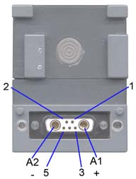
The "D" style connector (29) has a couple of large contacts which
are the terminals.
When looking at the battery connector with the long side of the "D"
at the top, the left large socket (A2) is the Negative (-) terminal
and the right large socket (A1) is the Positive (+) terminal.
The small sockets are numbered as follows:
1 = upper right
2 = upper left = thermistor
3 = lower right = thermistor
5 = lower left
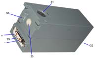
The plastic part (30) provides the latching action for the "1" metal
latching plate. A fuse (31) is marked T101 and there is a
spare fuse (32) on the rear face of the battery. The metal
thing (33) is a vent that lets gas out but does not let water in.
By using a piece of 3x5 card stock as an insulator and the stock
clips on my Maha C777Plus battery charger, the battery can be
charged. It's now reading 17 volts while on charge. Once
charged I'll discharge it using the Maha to see what the capacity is
now.
After 1 hour of charging 0.754 AH have been put into the battery.
Wireless For The Warrior Vol. 4 lists the battery capacity as 14.4
Volts 1.2 Amp Hours, which is a little more than 17 Watt
Hours. If the transmitter puts out 40 Watts and is 50%
efficient (I have not measured the current draw while transmitting)
then the current might be 5.5 Amps. The Amp Hour capacity of a
battery does not remain constant as the current is varied, but
decreases and the current is increased above the 20 hour rate.
For a 1.2 Amp Hour battery the 20 hour rate is 60 milliamps.
So instead of expecting to get 1.2 AH/ 5.5 A = 0.2 hours = 13
minutes time 2 for two batteries = 26 minutes, the actual capacity
of the batteries will be more like 5 or 10 minutes of transmit time
for both of them.
Note the fuse is rated for 10 Amps, probably correct for transmitter
use, but way too strong to protect the receiver from
mishandling. The receiver Synthesizer PCB that connects the
DB-25 Tx controller connector and the Tx interface connector as well
as supplying DC to the receiver is a 3 or 4 layer PCB with traces
that can carry about 0.4 amps. 10 amps will blow out the
traces.
Battery Charger
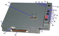 The
Chrager has two uses. One is to charge batteries and the other
is to supply DC to the transmitter.
The
Chrager has two uses. One is to charge batteries and the other
is to supply DC to the transmitter.
The battery charger can be powered by either a "12 Volt" source
connected to the Red and Black 5-Way binding posts (34) or from the
AC Mains power supply "M" using terminals (48) which will work with
inputs from 110 to 240 VAC.
The charger can charge one or two batteries in the 10 hour mode or
two batteries in the fast mode. The charger can charge the
batteries either through the H bar adapter or through the
transmitter.
So far I have not been able to get the B2 light (42) to come
on. I've tried connecting a single battery to both possible
locations and tried two batteries. The Fast Charge (38), 10
Hour charge (40) and B1 (41) lights work as you would expect.
Also have not been able to get any of the Power Check LEDs: Full
(45), OK (46) or Low (47) to come on. When the Power Check
button (44) is pressed it turns off charging.
On the big connector pin 12 is connected to pin 13 and pin 15 is
connected to pin 17 (ground). The two outside large
connections are A1 ground and A4 +14.0 Volts to power the
Transmitter, the other high current DC pins may be for
charging batteries when they are on the Transmitter.. Note
that high current DC pins are not used for charging batteries with
the H bar.
Mains AC Power Supply
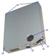 The line
cord connector (52) is the same as used for the brick power supply
common to lap top computers, I used the one from my Sony VIAO.
The fuse (53) and spare fuse (54) are nearby. There are four
captive screws (55) that allow attaching the Mains supply to the
battery charger.
The line
cord connector (52) is the same as used for the brick power supply
common to lap top computers, I used the one from my Sony VIAO.
The fuse (53) and spare fuse (54) are nearby. There are four
captive screws (55) that allow attaching the Mains supply to the
battery charger.
On the bottom of the Mains power supply are a couple of metal
contacts (56) that pass 14 VDC to the Battery Charger terminals
(48).
Note that the power supply is not strong enough to charge the
batteries and power the transmitter.
Configurations
I frimly believe that this system
has been designed to be as idiot proof as possible. In some
cases they have have used two methods to prevent making a wrong
connection. So any configuration that can be made is very
likley to be a valid one. The strings of capital letters in
the following titles are the ID letters of the components in the
setup. For example MCHBB is composed of the
Mains power supply, battery
Charger, "
H" connector bolck and two
Batteries.
MCTABBK Normal Use
If
the FS5000 was keept in the nice shipping boxes the Ni-Cad
batteries would be dead. The most logical way to use the
FS5000 is to have the A.C.
Mains
supply, battery
Charger,
Transmitter,
Antenna coupler and a couple
of
Batteries and the
accessory
Kit all
connected toghther. Since the battery Charger can charge the
batteries through the transmitter this would be the normal use
configuration. Every so often, say once a week (month,
quarter?) one of the batteries would be removed and discharged to
be sure there was no Ni-Cad memory problem. If just after
discharging one battery there was an emergency and the A.C. mains
power went down, the radio still would work from the other
battery. This is probably why there are two batteries.
The Accessory
Kit (my
letter for it) is designed to plug into the side of the receiver
and snap down onto the corner of the Charger. When this is
done the void under the accessory Kit, the Mains supply + charger
and the Receiver is about 45 mm high, 125 mm wide (150 mm
including a DB-25m connector) and 100 mm deep. So these
might the the dimensions of the missing Transmitter Controller.
TA23 Installing the Metal Locking Plates
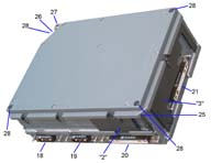
Here the Antenna Coupler has been connected
to the Transmitter after first installing the "2" and "3" metal
locking plates. The Receiver can be locked using the "2"
plate and the combined Mains supply and Battery Charger can be
locked using the "3" plate.
Note the locking plates need to
be installed prior to using screws to attach the top and bottom
parts.
TCAMR23 AC Mains powered Receive -
Transmit

This is an configuration combines the
Transmitter, Antenna Coupler, Mains power supply, Battery charger
and Receiver, latched together using screws for up-down connection
and metal plates "2" and "3" for horizontal connection.
This would be used for a transceiver system that's powered from
the AC mains. The Charger is not being used for charging or
any electrical purpose, but just to assist the metal latching
plates to hold every thing together.
Note that this configuration uses the (21) connector, that's the
big one on the side of the transmitter with 17 sockets and 4 high
current DC positions, to connect to the Charger. This means
that the (21) connector is NOT available for connecting to the
missing transmitter controller. But the (6) connector, the
standard DB-25 connector on the receiver, is available to control
the system.
This has an interesting implication. To get to the
configuration TARBB112 starting from the TCAMR23 setup, the Mains
PS and Charger are removed by sliding the "3" locking plate back
and then adding a couple of batteries (the Transmitter and Antenna
Coupler need to be separated to get the two "1" locking plates
installed. Note that in the TARBB112 Battery powered
configuration there's a space to connect the missing Transmitter
controller. A conjecture is that when using the system in
the filed with battery power the missing controller is needed, but
when using the system from a mains power supply the missing
controller is not needed and something needs to be connected to
the DB-25 connector (6) on the Receiver.
A quick check with a Ohm meter shows the the DB-25 connector has
pins 23 and 25 tied to chassis ground. This is NOT
compatable with the standard pin out for a PC serial (COM)
port. So this conector has some special pin out.
TARBB112 Battery Powered Receive
Transmit
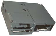
The two Batteries and Receiver are all on the Transmitter front
panel held there by the "1", "1" and "2" metal locking plates.
On the right face there are two ways more units might be
attached. The Transmitter Controller would still fit on the
Receiver using the locking lever. Something else, or maybe
the Transmitter Controller using a different face could be
attached to the Transmitter using the "3" metal locking plate.
MCHBB Battery Charging from A.C. Mains
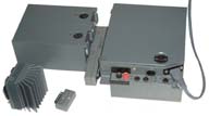
Charging
the batteries from the A.C. mains is done using the mains supply
"M" stacked on top of the Battery charger "C". The
connecting block "H" joins the two batteries to the charger.
When charging batteries it's handy to have at least one of the "S"
State of Charge indicators as well as the "F" discharger
handy. Note that the two batteries have different
serial numbers (3186 & 5186 in my cae) and likewise the two
State of Charge indicators have serial numbers that match the
battery serial numbers. This way each system part has a
unique ID+serial number.
Discharging the two batteries on the Maha gives the following
data:
Time
min
B-5186
|
mAH
|
Volts
|
Time
min
B-3186 |
mAH |
Volts |
28
|
158
|
15.1
|
0
|
0
|
16.2
|
53
|
297
|
14.7
|
49
|
274
|
14.5
|
111
|
623
|
14.4
|
107
|
602
|
14.3
|
147
|
823
|
14.1
|
131
|
735
|
14.2
|
167
|
935
|
13.8
|
167
|
939
|
13.8
|
176 end
|
985 |
13.6 |
175
|
982
|
12.7
|
After the Maha had finished discharging B-3186 the "S"
battery checker was installed and it's LED glowed Green. But
when the "F" discharger is plugged onto B-3186 it's green LED
flashes for a fraction of a second and then is dark. The "S"
tester is off at 12.0 Volts and on bright at 13.5 Volts.
After leaving a couple of batteries on the charger overnight, in
the morning the A.C. Mains supply LED is green and the FULL (45)
led is green, all other LEDs have turned off, i.e. charging has
stopped and neither battery is being charged.

The "F" battery discharger has a male type
connector to mate with the battery female connector. It has
it's own "1" metal latching plate to allow fixing it to the
battery being discharged. This would be convenient for field
use where they could be mated and then put in a pack sack without
worry about them coming apart.
RHB Portable
Receiver
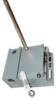
This receiver is composed of one battery, the
"H" connector block and receiver. The earphone and
telescoping antenna from the accessory kit are used. It does
not appear that any of the metal locking plates can be used so
this system can only be used on a flat surface, not at all a field
portable configuration. This may have been used for testing.
I can pickup a local AM station and WWV, but need to collapse the
antenna and move away from my computer.
With the receiver set for 3000 Hz bw, delta freq centered, freq
20000. HP 8648A sig gen set for 20.00000 MHz (Fc), SIN
modulation and varying the modulation frequency the tuning LEDs on
the receiver switch so that "+" is on for 1.1 kHz and above and "_"
for 1 kHz and below. The earphone sounds tones from about 600
Hz to 2.7 kHz. With the sig gen RF off the "-" LED is on mostly, but
sometimes noise causes them both to flicker.
Using just a CW carrier from the sig
gen both LEDs are off at Fc + 880 Hz, the "-" LED is on at Fc+1010
Hz through Fc + 1070 Hz then the "+" LED is on at Fc +1080 Hz
through Fc + 3320 Hz where noise is heard and the "+" LED
flickers, higher RF frequency is out of the receiver
passband. So it looks like the "+" and "-" LEDs are fed from
a crossover filter centered at a nominal 1 KHz above the tuned
frequency (i.e. USB). Tuning the sig gen below 20 MHz
produces no receiver output, i.e. it not an AM receiver.
Links
YouTube
FS 5000 receiver demo -
Cold War Spy Radio - manual operation, no control box,
would have been better to use coax input for antenna or an HF
transformer to simulate the impedance of the whip antenna.
Modulator
Class 332 is Modulators, 375
is Pulse or Digital Communications, 455 is Telecommunications
While none of these patents is
directly related to the FS5000 Modulator, they might helping
understanding it.
4626803 Apparatus for providing a carrier signal with two
digital data streams I-Q modulated thereon Dec 2, 1986
332/151;
375/298
4540958
Zero IF frequency-modulator Sep 10, 1985
332/128; 455/42; 455/102
4438413
Serial minimum shift keyed modulator including notch and bandpass
filters March 20, 1984
332/100; 375/305
Patents where
Siemens
is the assignee & the Class contains 332 -
4617537 Method for digital quadrature amplitude modulation
Oct 14, 1986
332/151;
332/108;
375/261 - Quadrature Amplitude Modulation (QAM)
4003002
Modulation and filtering device Jan 11, 1977
332/185;
332/170; 375/296; 375/301
4086536
Single sideband transmitter apparatus Apr 25, 1978
455/109;
332/170; 455/118
4433310
Modulator-demodulator for four level double amplitude
modulation on quadrature carriers Feb 21, 1984
332/151;
329/306; 375/269; 375/343
5418818 Digital signal processor exciter May 23, 1995
375/264;
375/216; 375/224; 375/356; 455/92; 455/102; 455/118; 455/503
4843613
Digitally implemented modulators June 27, 1989
375/295;
332/117; 375/269; 375/303; 375/308 - includes some
calculations of PROM sizes for given conditions. An
audio passband modulator.
4613976
Constant envelope offset QPSK modulator Sep 23, 1986
375/279;
332/103; 375/281; 375/308 - Fig 1 uses two ROMs, one for I
and one for Q, followed by D/A converters.
Patents
Modulation
4780884
Suppressed
double-sideband communication system, Peter
D. Karabinis (AT&T),
Mar 3, 1986, 375/261,
375/270, 370/206, 375/301
4730345
Vestigial
sideband signal decoder, Howard
C. Reeve, III (AT&T),
Apr 4, 1986, 375/321,
327/552
5663773
Demodulator
for a complex-value vestigial sideband signal, Heinz
Goeckler (Ant
Nachrichtentechnik Gmbh), Dec 16, 1994,
348/726, 348/E05.113, 348/736, 329/357, 455/337
Antenna Coupler
Class
333
Wave Transmission Lines and Networks
Miscellaneous
4162446 Transceiver with only one reference frequency
July 24, 1979 455/77;
333/165; 455/83; 455/84 -
H.F. radio
Back to Brooke's Products
for Sale, Crypto, Crypto
Machines, Brooke's Military Information,
Home page
[an error occurred while processing this directive] page created 23 Oct.
2004.

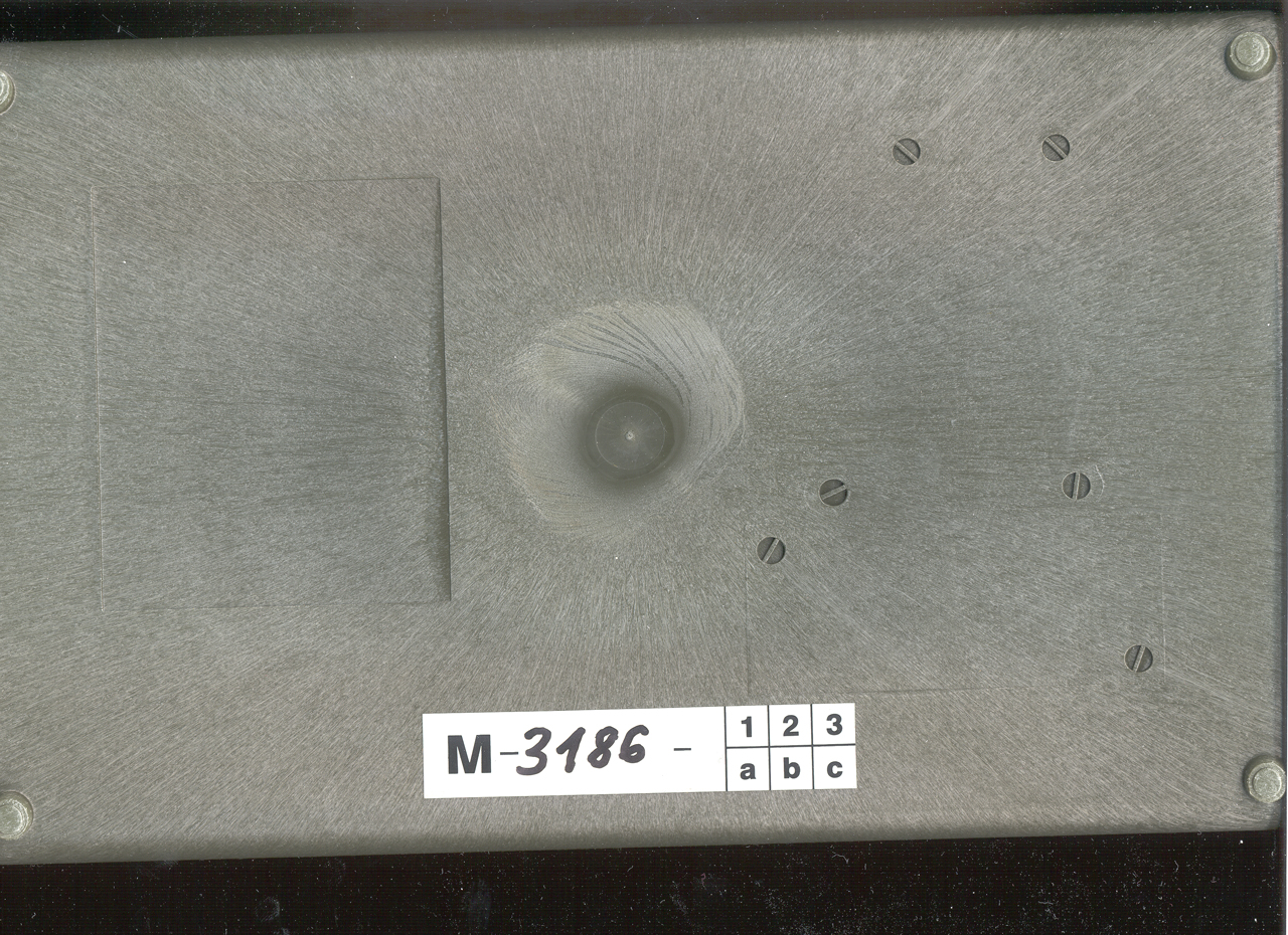 All the large box tops have a shallow
80x100 mm depression where a label could be pasted. In
addition there are three places where lettering could be molded
into the plastic, but these have been filled with blank plates
using a couple of single slot "-" flat head scrws for each
one. The labels could have been 95x42, 10x70 and 10x45 mm
All the large box tops have a shallow
80x100 mm depression where a label could be pasted. In
addition there are three places where lettering could be molded
into the plastic, but these have been filled with blank plates
using a couple of single slot "-" flat head scrws for each
one. The labels could have been 95x42, 10x70 and 10x45 mm 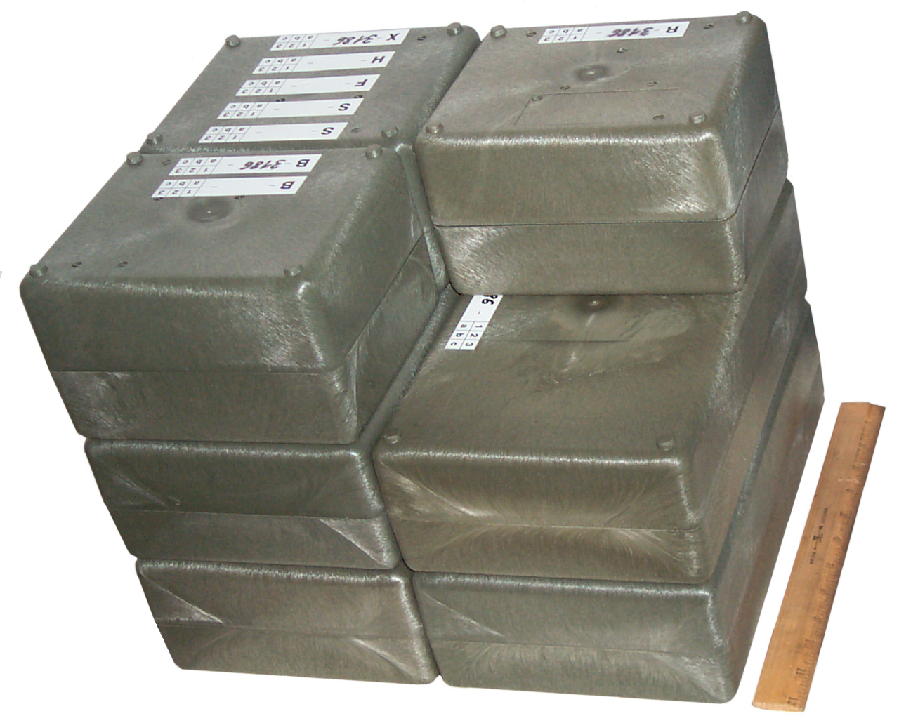
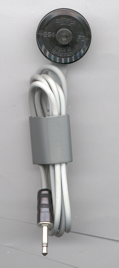
 Plastic flat
blade (-) screwdriver marked Siemens
Plastic flat
blade (-) screwdriver marked Siemens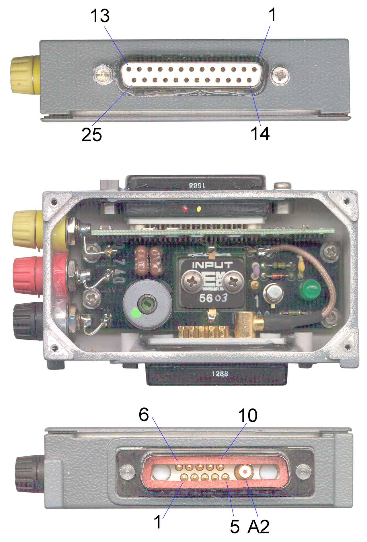 The lid screws are #1
Phillips and were installed with Locktite so plenty of down
force is needed to keep from striping the (+) mating
notches.
The lid screws are #1
Phillips and were installed with Locktite so plenty of down
force is needed to keep from striping the (+) mating
notches.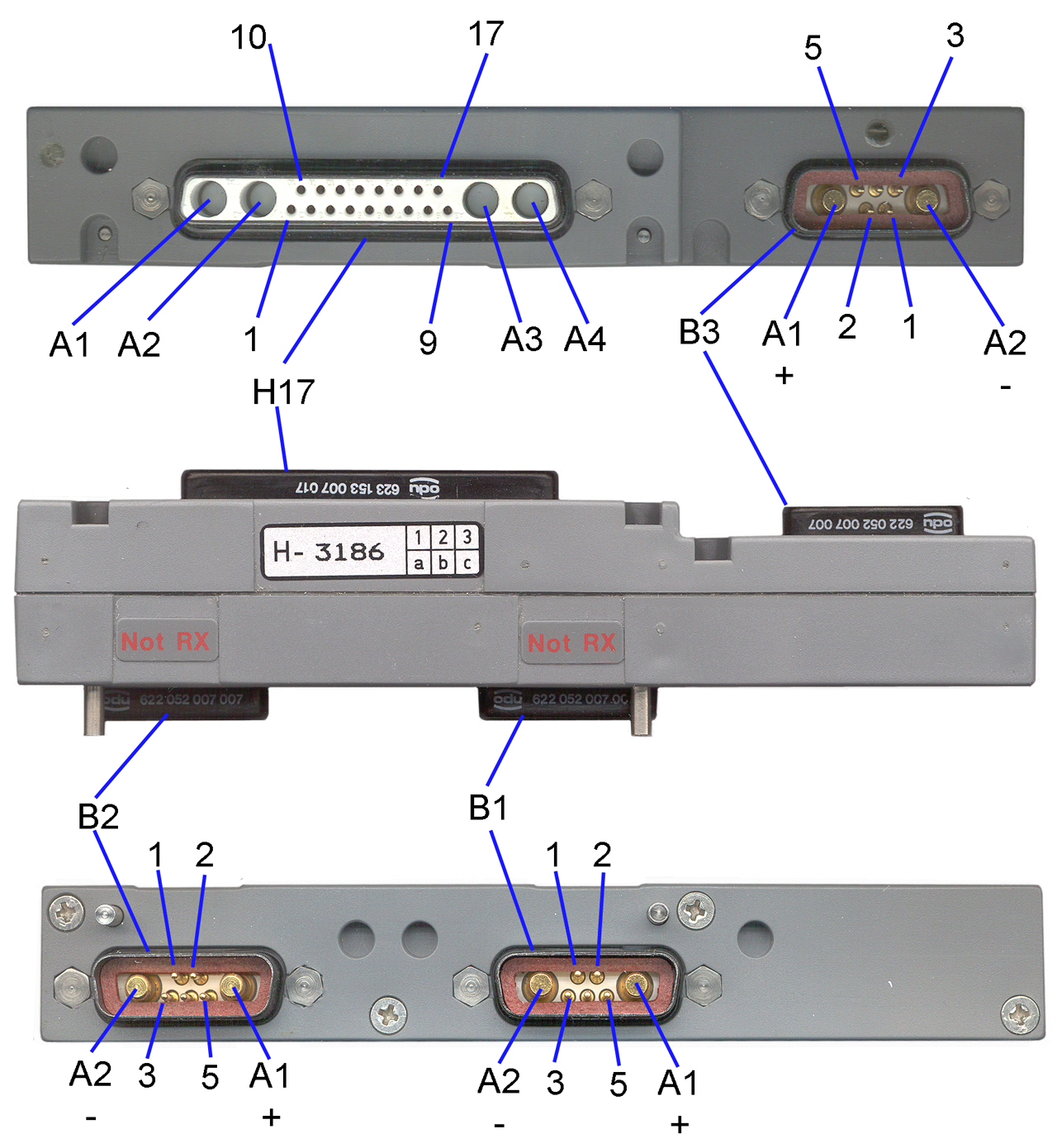 There are two different uses
for the H bar. When used with the battery charger-DC
power supply it provides the means to connect one or two
batteries to the charger. When used with the
Receiver it allows a single battery to power the Receiver.
There are two different uses
for the H bar. When used with the battery charger-DC
power supply it provides the means to connect one or two
batteries to the charger. When used with the
Receiver it allows a single battery to power the Receiver. On a 45 degree sloping small panel,
left to right:
On a 45 degree sloping small panel,
left to right: On a side there's a DB-39 shell
(16) with 17 male pins and 4 female coax connectors.
This connector will mate to the one on the "H" 4 connector
block in the "S,X" packing box. The "H" bar is a way to
connect one battery to the Receiver for receive only
use. This connector also mates to one on the
Transmitter, but not to the other connector on the the
transmitter that appears to be similar, not becasue it's the
wrong connector, but because there are metal pins the prohibit
making that connection. This design seems fool proof.
On a side there's a DB-39 shell
(16) with 17 male pins and 4 female coax connectors.
This connector will mate to the one on the "H" 4 connector
block in the "S,X" packing box. The "H" bar is a way to
connect one battery to the Receiver for receive only
use. This connector also mates to one on the
Transmitter, but not to the other connector on the the
transmitter that appears to be similar, not becasue it's the
wrong connector, but because there are metal pins the prohibit
making that connection. This design seems fool proof.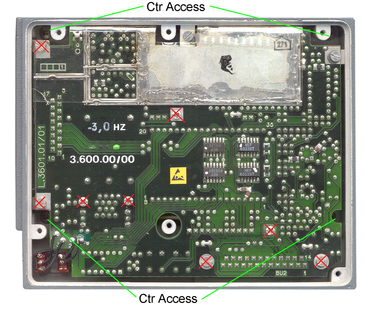 On the PCB in the bottom of the receiver
between pins 3 and 4 of the 4 coax connector (16) there are
small drops of black and green dielectric that appear to be
capacity tweaking. Just above this nest of traces is the
stamped message: "-3,0 Hz". These dots are some
type of revision marking, not tweaking. They appear on
many of the other boards in close proximity to the long white
silkscreen number that's the board ID, typically a group of 3
dots, probably using reisitor color code, so black black green
would be 005.
On the PCB in the bottom of the receiver
between pins 3 and 4 of the 4 coax connector (16) there are
small drops of black and green dielectric that appear to be
capacity tweaking. Just above this nest of traces is the
stamped message: "-3,0 Hz". These dots are some
type of revision marking, not tweaking. They appear on
many of the other boards in close proximity to the long white
silkscreen number that's the board ID, typically a group of 3
dots, probably using reisitor color code, so black black green
would be 005.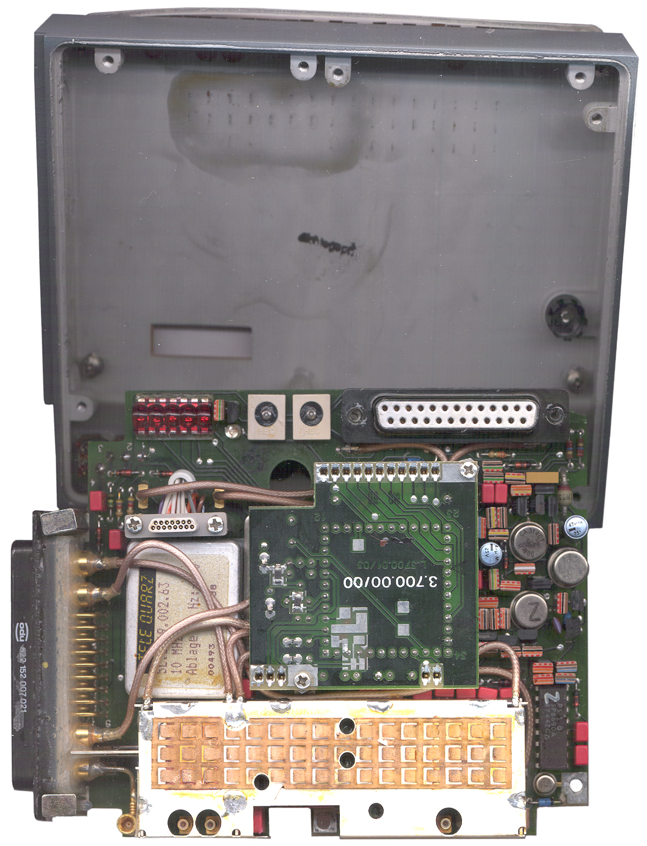 There is a 10 MHz Tele Quarts OCXO marked
- 3 Hz.
There is a 10 MHz Tele Quarts OCXO marked
- 3 Hz.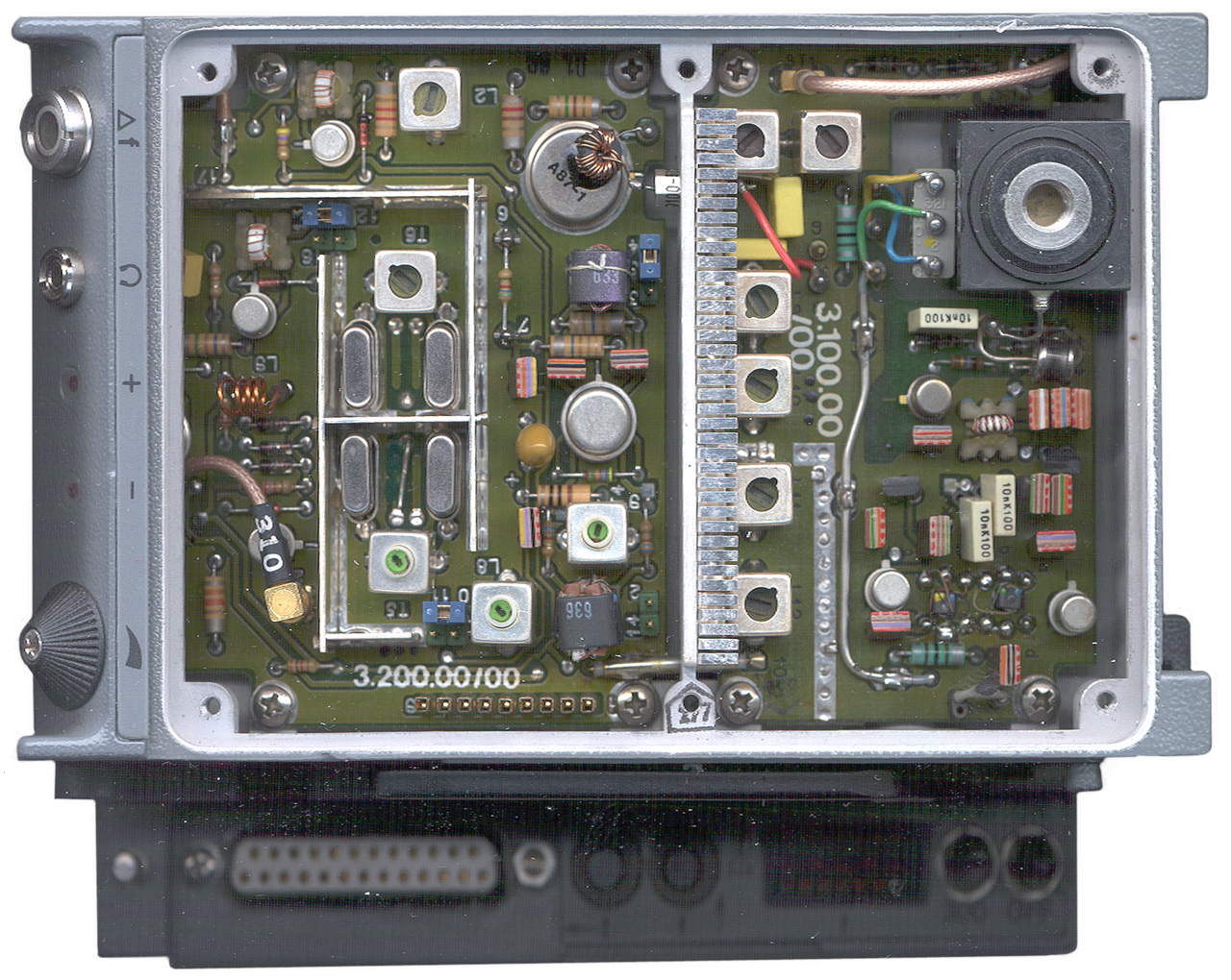 The top cover also has TEMPEST type
shielding. There are two compartments on the top
side.
The top cover also has TEMPEST type
shielding. There are two compartments on the top
side. 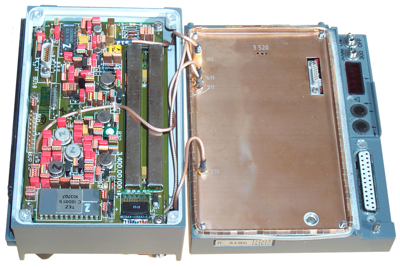 After
the bottom cover is removed and the 4 captive screws down behind
the notches in the bottom PCB are backed out the receiver case can
be split open. Connecting the top and bottom portions of the
receiver are 4 coax cables and a miniature DB-15 pin connector
that may be identical to the one used for the SVM-68 to radio connection. The coax
supplying the signal from the antenna tuner is marked 101 on the
bottom half of the receiver. The LO comes up from the bottom
through the 210 coax. It's not clear what the 311 and 411
coax cables are carrying.
After
the bottom cover is removed and the 4 captive screws down behind
the notches in the bottom PCB are backed out the receiver case can
be split open. Connecting the top and bottom portions of the
receiver are 4 coax cables and a miniature DB-15 pin connector
that may be identical to the one used for the SVM-68 to radio connection. The coax
supplying the signal from the antenna tuner is marked 101 on the
bottom half of the receiver. The LO comes up from the bottom
through the 210 coax. It's not clear what the 311 and 411
coax cables are carrying.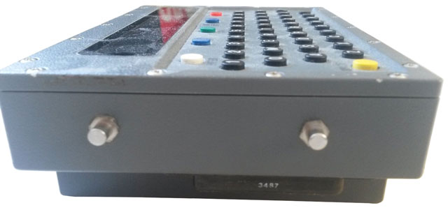
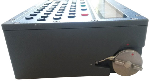
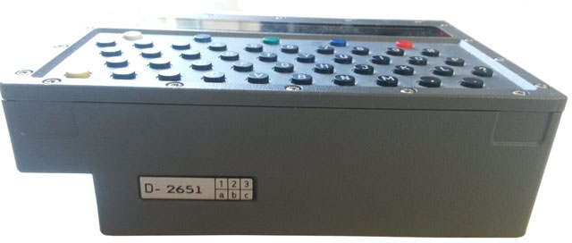
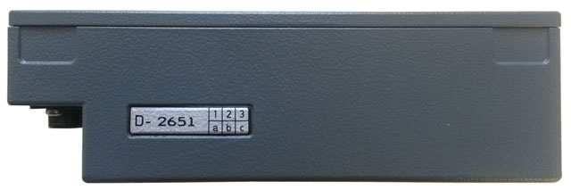
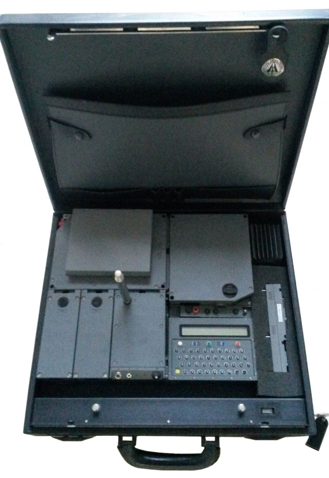
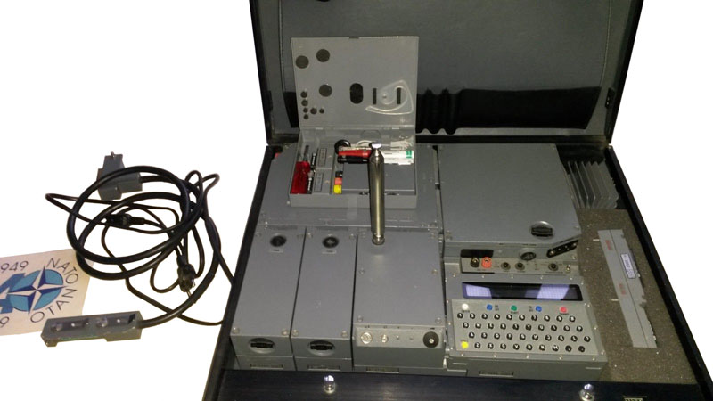
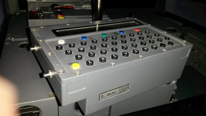
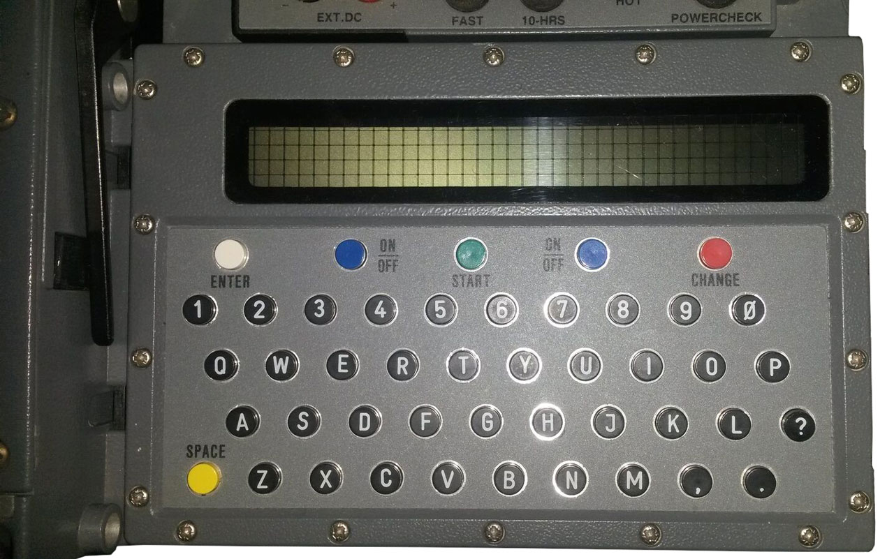
 When
the following modules are combined: Transmitter, Antenna coupler,
Mains power supply, battery Charger, Battery, Battery Receiver and
accessory Kit there is a space under the accessory Kit and in
front of the Mains power supply and charger and to the right of
the Receiver where the Transmitter Controller fits.
When
the following modules are combined: Transmitter, Antenna coupler,
Mains power supply, battery Charger, Battery, Battery Receiver and
accessory Kit there is a space under the accessory Kit and in
front of the Mains power supply and charger and to the right of
the Receiver where the Transmitter Controller fits.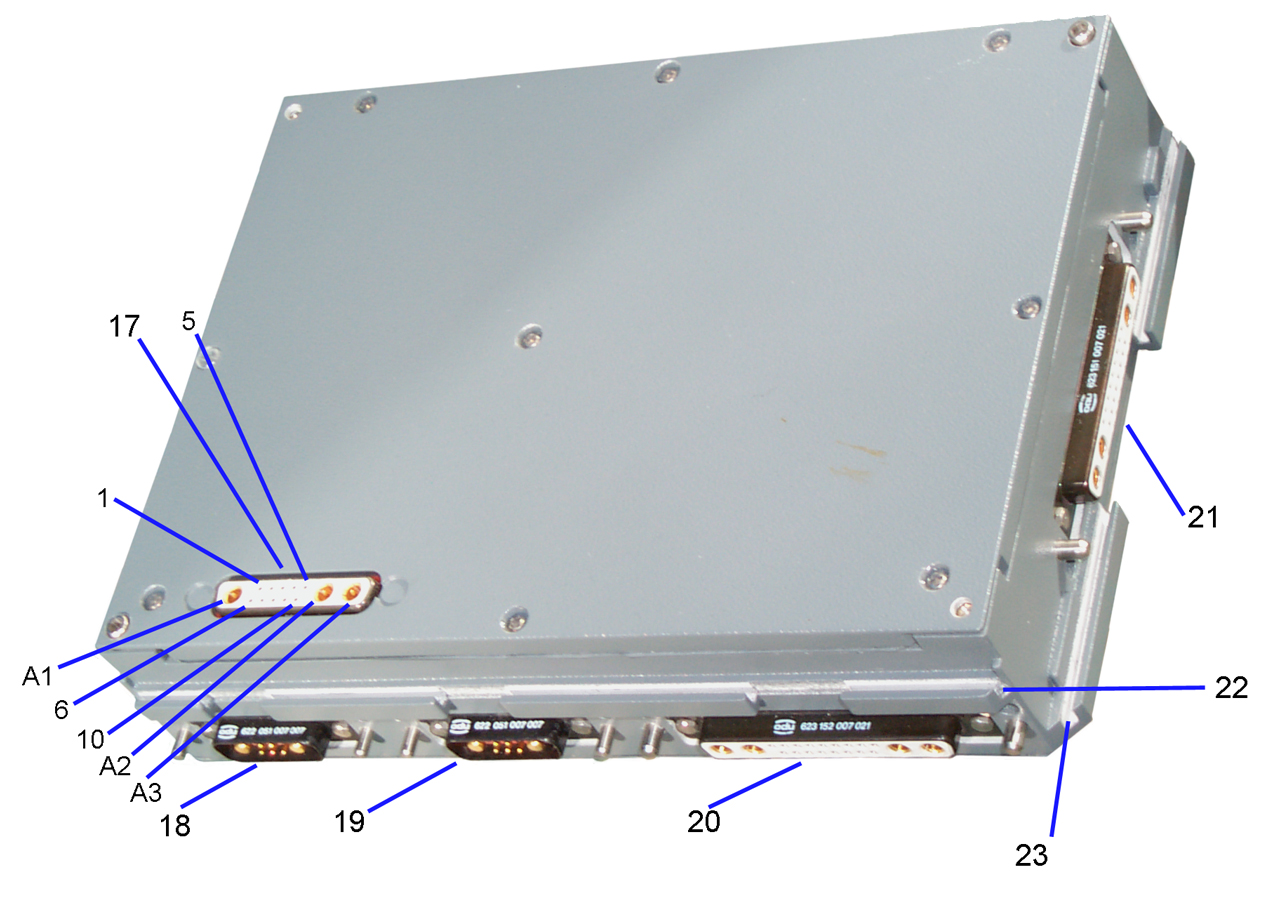 This
transmitter uses digital In phase and Quadrature ( I&Q)
modulation methods which are very much more sophisticated than the
more common RTTY modes used on H.F. The mode is likley
either QPSK (Quadrature Phase Shift Keying) or OQPSK (Offset -QPSK,
where no 180 degree changes are made). The power output can be
adjusted using the "PO" pot near the final amplifier stage on the
bottom PCB. With the factory setting the CW output is about 40
Watts.
This
transmitter uses digital In phase and Quadrature ( I&Q)
modulation methods which are very much more sophisticated than the
more common RTTY modes used on H.F. The mode is likley
either QPSK (Quadrature Phase Shift Keying) or OQPSK (Offset -QPSK,
where no 180 degree changes are made). The power output can be
adjusted using the "PO" pot near the final amplifier stage on the
bottom PCB. With the factory setting the CW output is about 40
Watts.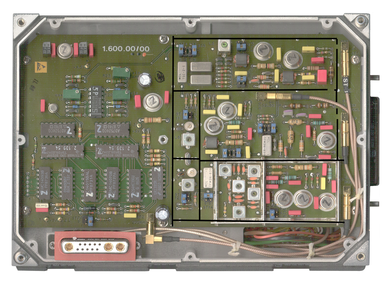 One
side has a number of ICs. These include a couple of 28L22
PROMs wiich are arranged as 256 bytes and next to these are a couple
of AD7524 8 bit ADCs. They are not fast enough for RF
synthysis, but would be great for an I-Q modulator. Next to
these is a SE5514N Quad comparator and from this there is a PCB top
trace labeled SIN COS that ends near the MCL TSC-2-1 two way
splitter and a couple of TSM-1 mixers. This is for sure an I
& Q modulator. These are fed from the fixed 50.0 MHz LO
and the 50 - 80 MHz variable LO after amplification with the Avantek
amps.
One
side has a number of ICs. These include a couple of 28L22
PROMs wiich are arranged as 256 bytes and next to these are a couple
of AD7524 8 bit ADCs. They are not fast enough for RF
synthysis, but would be great for an I-Q modulator. Next to
these is a SE5514N Quad comparator and from this there is a PCB top
trace labeled SIN COS that ends near the MCL TSC-2-1 two way
splitter and a couple of TSM-1 mixers. This is for sure an I
& Q modulator. These are fed from the fixed 50.0 MHz LO
and the 50 - 80 MHz variable LO after amplification with the Avantek
amps. 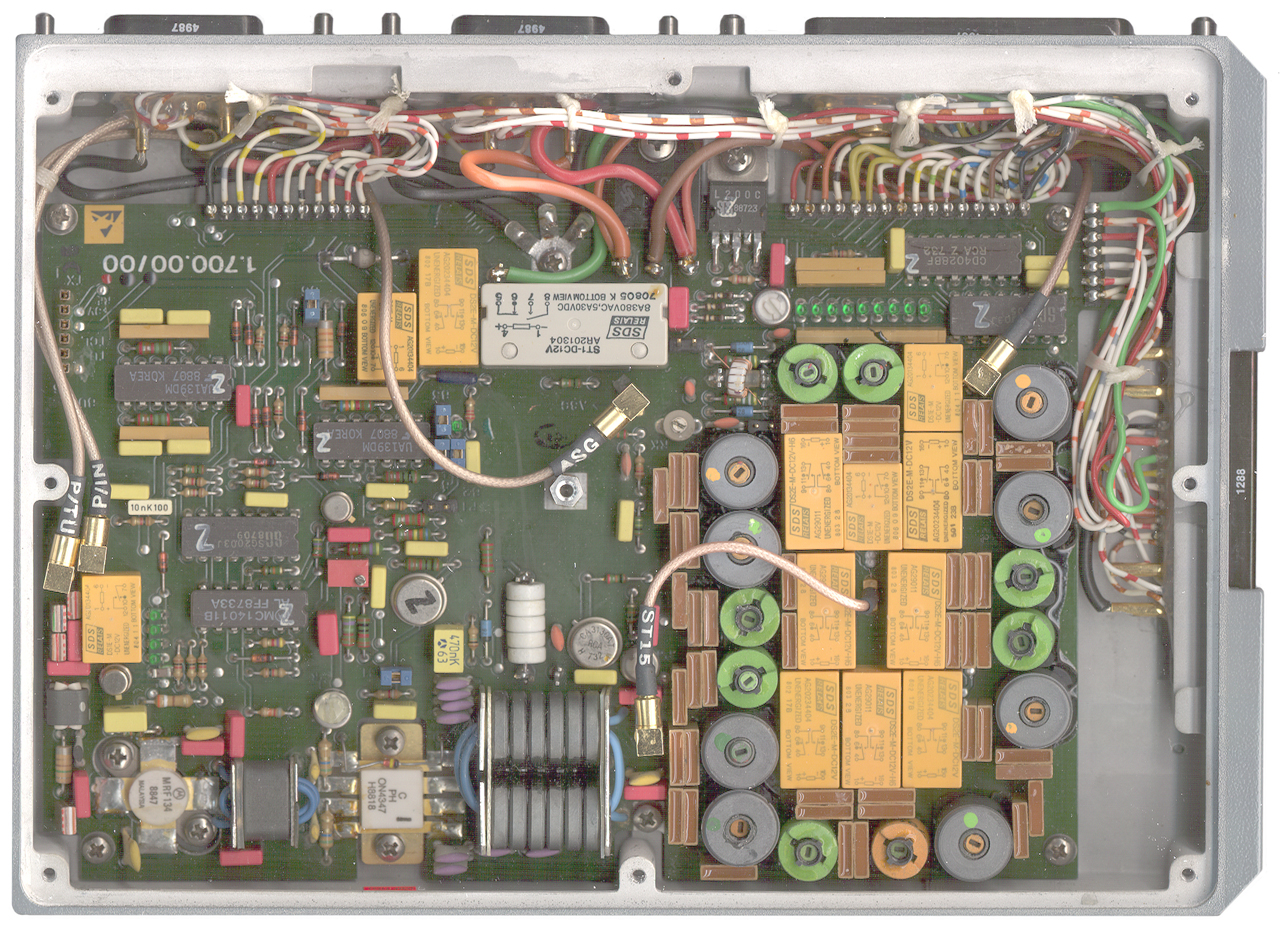 The RF
power amp consists of an MRF134 (about 3 Watts out) driving a small
transformer then an ON4347 driving a larger transformer then a coax
marked ST15 going to the center of a filter bank using 9 each DPDT
relays 16 inductors and 48 caps. There's also what may
be a high VSWR detector. Beside the filter bank there a string
of 9 small green LEDs.
The RF
power amp consists of an MRF134 (about 3 Watts out) driving a small
transformer then an ON4347 driving a larger transformer then a coax
marked ST15 going to the center of a filter bank using 9 each DPDT
relays 16 inductors and 48 caps. There's also what may
be a high VSWR detector. Beside the filter bank there a string
of 9 small green LEDs.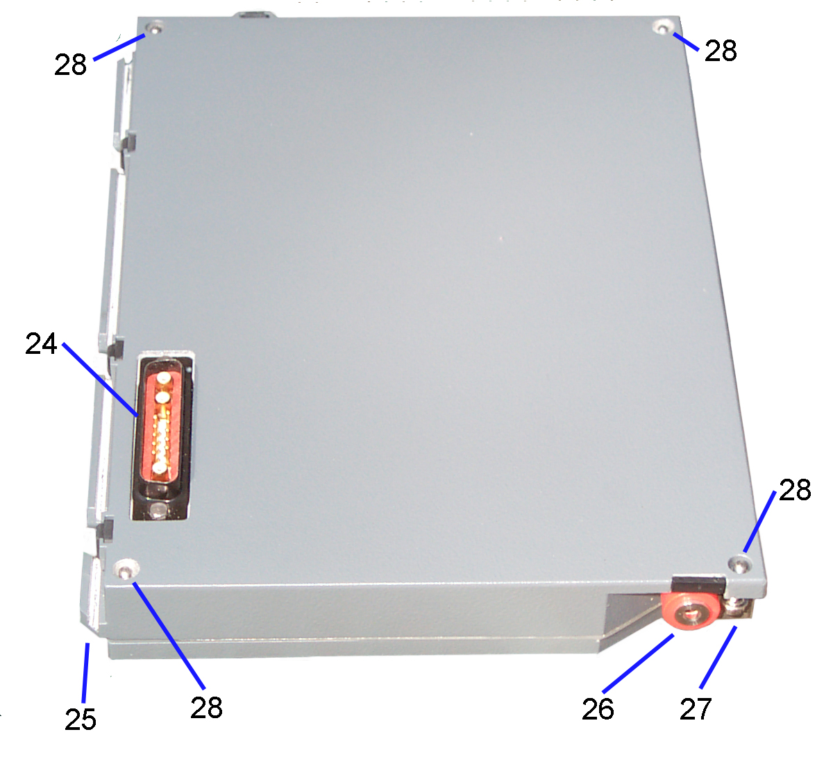 The
Antenna Auto Coupler can be placed on top of the transmitter.
It attaches to the top of the Transmitter using 4 screws (28).
The transmit antenna plugs into the Red banana socket (26).
The ground connection is the metal block (27) next to the red
antenna jack.
The
Antenna Auto Coupler can be placed on top of the transmitter.
It attaches to the top of the Transmitter using 4 screws (28).
The transmit antenna plugs into the Red banana socket (26).
The ground connection is the metal block (27) next to the red
antenna jack. 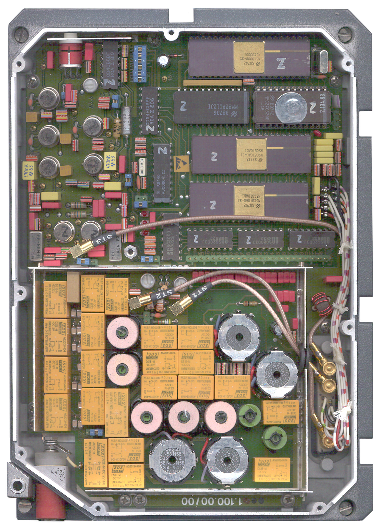
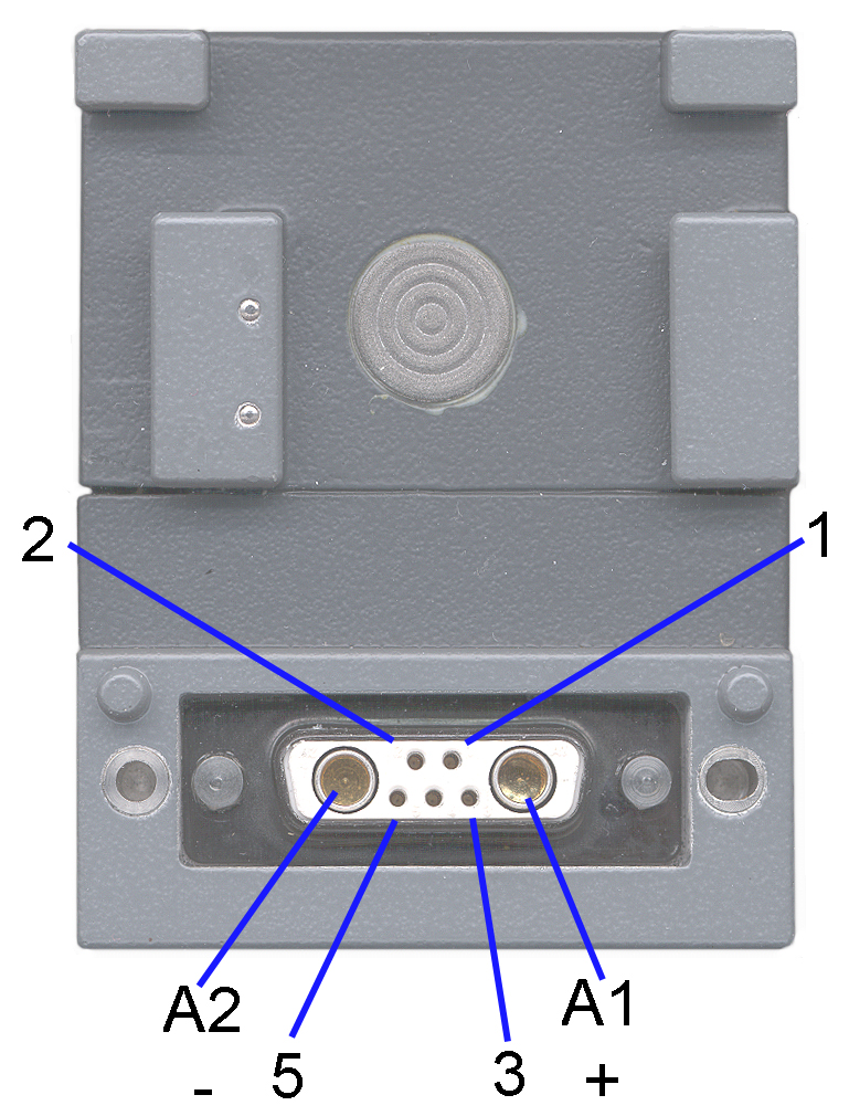
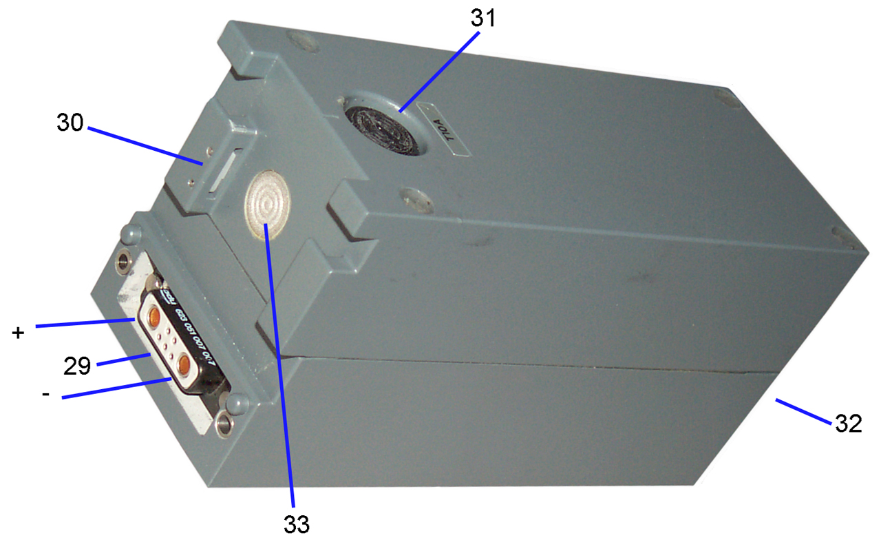
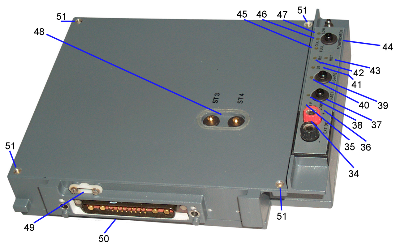 The
Chrager has two uses. One is to charge batteries and the other
is to supply DC to the transmitter.
The
Chrager has two uses. One is to charge batteries and the other
is to supply DC to the transmitter.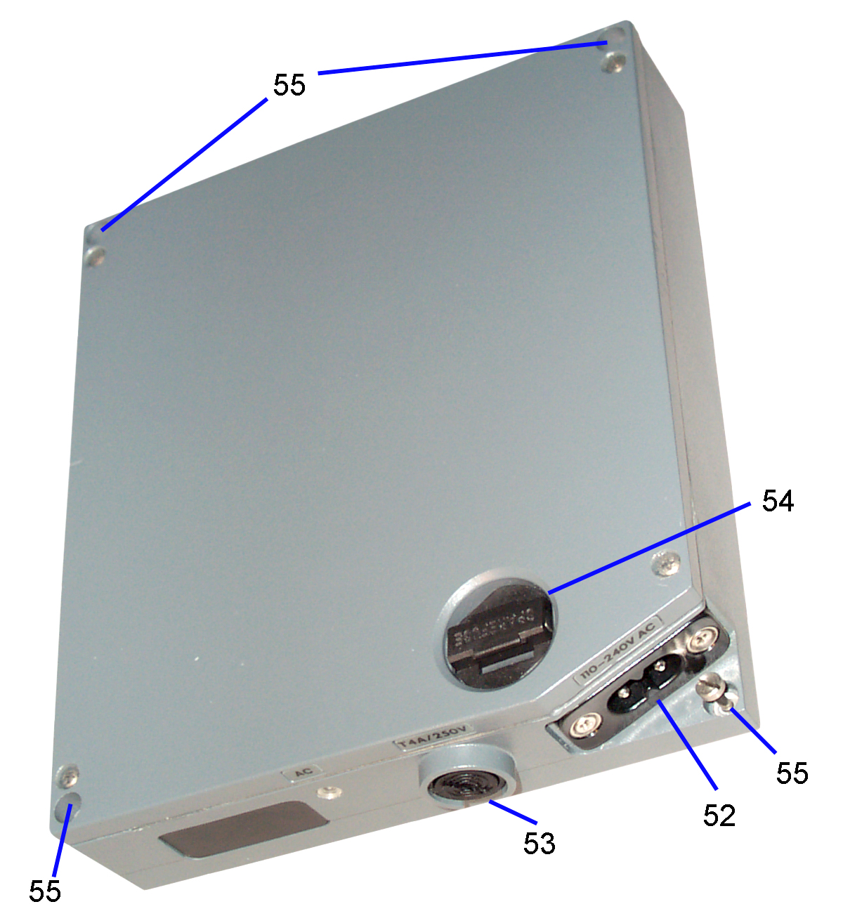 The line
cord connector (52) is the same as used for the brick power supply
common to lap top computers, I used the one from my Sony VIAO.
The fuse (53) and spare fuse (54) are nearby. There are four
captive screws (55) that allow attaching the Mains supply to the
battery charger.
The line
cord connector (52) is the same as used for the brick power supply
common to lap top computers, I used the one from my Sony VIAO.
The fuse (53) and spare fuse (54) are nearby. There are four
captive screws (55) that allow attaching the Mains supply to the
battery charger.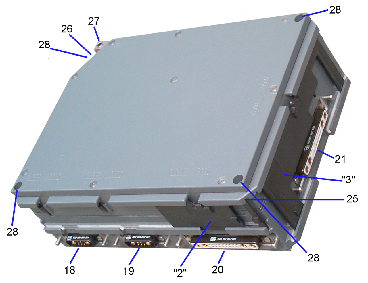 Here the Antenna Coupler has been connected
to the Transmitter after first installing the "2" and "3" metal
locking plates. The Receiver can be locked using the "2"
plate and the combined Mains supply and Battery Charger can be
locked using the "3" plate.
Here the Antenna Coupler has been connected
to the Transmitter after first installing the "2" and "3" metal
locking plates. The Receiver can be locked using the "2"
plate and the combined Mains supply and Battery Charger can be
locked using the "3" plate. 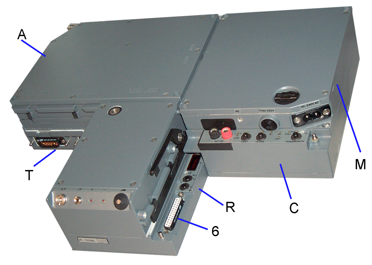 This is an configuration combines the
Transmitter, Antenna Coupler, Mains power supply, Battery charger
and Receiver, latched together using screws for up-down connection
and metal plates "2" and "3" for horizontal connection.
This is an configuration combines the
Transmitter, Antenna Coupler, Mains power supply, Battery charger
and Receiver, latched together using screws for up-down connection
and metal plates "2" and "3" for horizontal connection.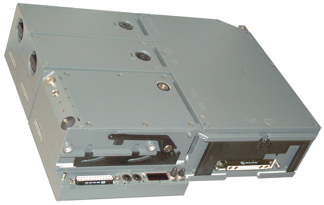
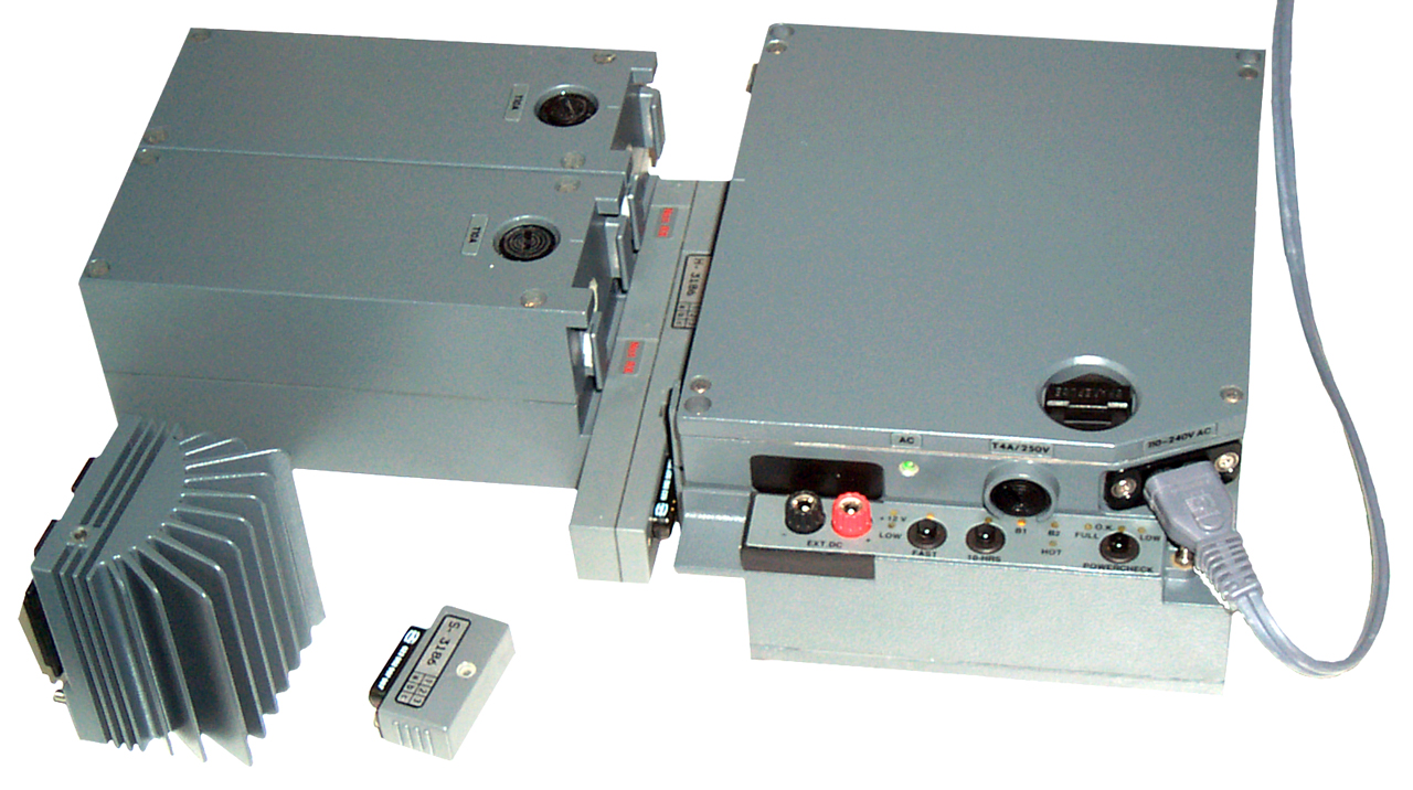 Charging
the batteries from the A.C. mains is done using the mains supply
"M" stacked on top of the Battery charger "C". The
connecting block "H" joins the two batteries to the charger.
When charging batteries it's handy to have at least one of the "S"
State of Charge indicators as well as the "F" discharger
handy. Note that the two batteries have different
serial numbers (3186 & 5186 in my cae) and likewise the two
State of Charge indicators have serial numbers that match the
battery serial numbers. This way each system part has a
unique ID+serial number.
Charging
the batteries from the A.C. mains is done using the mains supply
"M" stacked on top of the Battery charger "C". The
connecting block "H" joins the two batteries to the charger.
When charging batteries it's handy to have at least one of the "S"
State of Charge indicators as well as the "F" discharger
handy. Note that the two batteries have different
serial numbers (3186 & 5186 in my cae) and likewise the two
State of Charge indicators have serial numbers that match the
battery serial numbers. This way each system part has a
unique ID+serial number.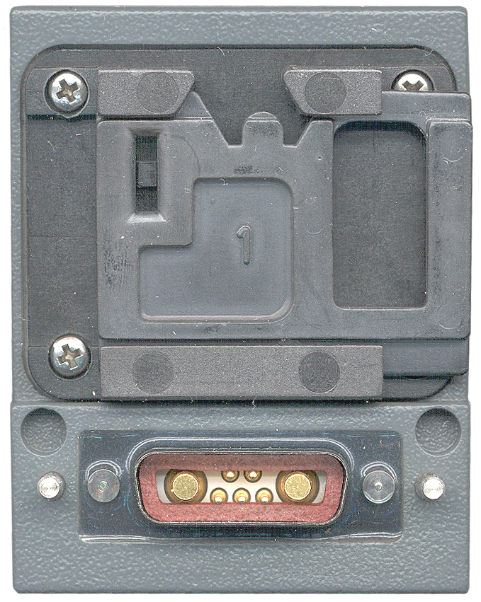 The "F" battery discharger has a male type
connector to mate with the battery female connector. It has
it's own "1" metal latching plate to allow fixing it to the
battery being discharged. This would be convenient for field
use where they could be mated and then put in a pack sack without
worry about them coming apart.
The "F" battery discharger has a male type
connector to mate with the battery female connector. It has
it's own "1" metal latching plate to allow fixing it to the
battery being discharged. This would be convenient for field
use where they could be mated and then put in a pack sack without
worry about them coming apart.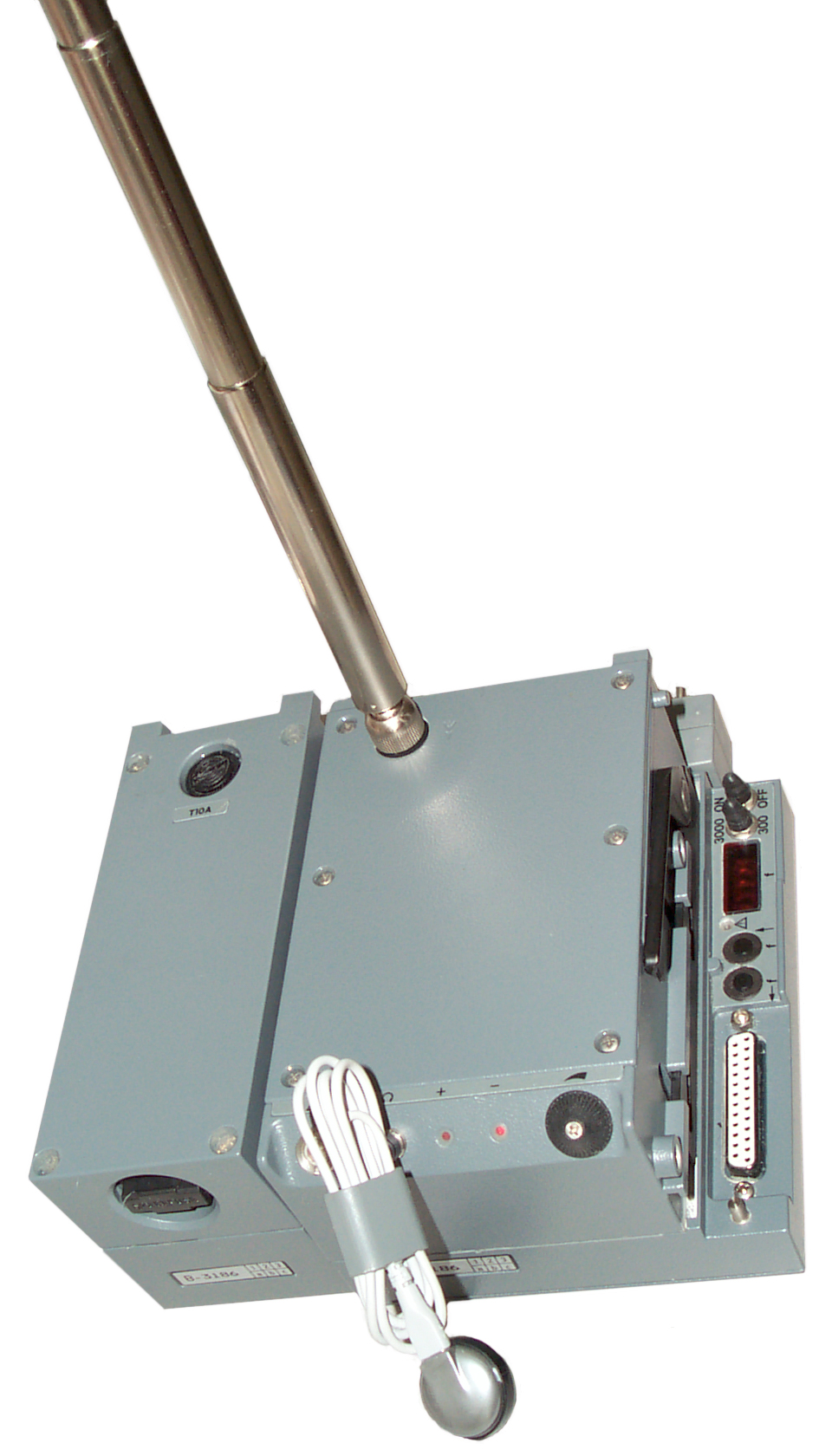 This receiver is composed of one battery, the
"H" connector block and receiver. The earphone and
telescoping antenna from the accessory kit are used. It does
not appear that any of the metal locking plates can be used so
this system can only be used on a flat surface, not at all a field
portable configuration. This may have been used for testing.
This receiver is composed of one battery, the
"H" connector block and receiver. The earphone and
telescoping antenna from the accessory kit are used. It does
not appear that any of the metal locking plates can be used so
this system can only be used on a flat surface, not at all a field
portable configuration. This may have been used for testing.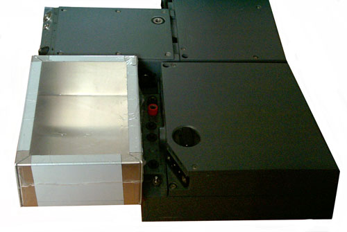
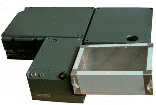
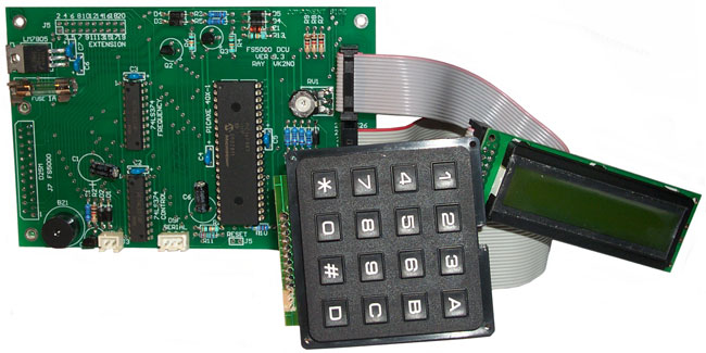
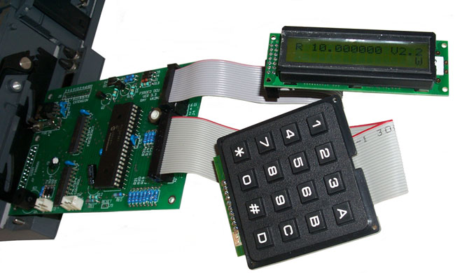